
Graphene detector and design method based on DC bias

A DC bias, graphene technology, applied in instruments, measuring devices, measuring current/voltage, etc., can solve the problem of low detection efficiency of graphene, and achieve the effect of good detection effect, stable operation and high detection efficiency.

Active Publication Date: 2021-03-30
CHENGDU UNIVERSITY OF TECHNOLOGY
View PDF4 Cites 0 Cited by
  • Summary
  • Abstract
  • Description
  • Claims
  • Application Information

AI Technical Summary

Problems solved by technology

[0005] The purpose of the present invention is to provide a solution to the above problems, improve the low efficiency of graphene detection, low cost, simple circuit structure, and good detection effect based on graphene detector and design method under DC bias

Method used


Image

  • Graphene detector and design method based on DC bias
  • Graphene detector and design method based on DC bias
  • Graphene detector and design method based on DC bias

Examples


Embodiment 1

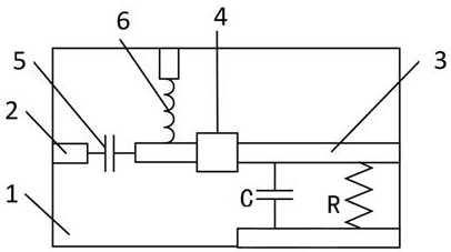
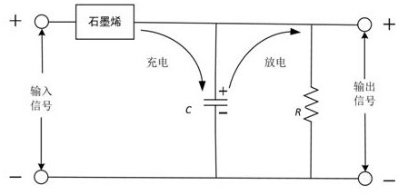
[0032] Embodiment 1: see Figure 1 to Figure 4 , a graphene detector based on DC bias, including a cavity, a signal input terminal 2, a signal output terminal 3, a graphene frequency doubler substrate in the cavity, and the graphene frequency doubler substrate includes a high-frequency medium The substrate 1 and the graphene 4 arranged thereon, the front end and the rear end of the graphene 4 are respectively connected to the signal input terminal 2 and the signal output terminal 3 through a microstrip line, and the signal input terminal 2 is used for external modulation signal, The modulation signal includes a low frequency signal f L and high frequency signal f H ;

[0033] Also includes an RC low-pass filter, the RC low-pass filter includes a filter main body, a signal transmission terminal and a ground terminal, the filter resistance of the filter main body is R, the filter capacitor is C, and 1 / f L CH C>>R, the signal transmission end is located on the microstrip line ...

Embodiment 2

[0037]Embodiment 2: A graphene detector based on DC bias, comprising a cavity, a signal input end 2, a signal output end 3, and a graphene frequency multiplier substrate in the cavity, wherein the graphene frequency multiplier substrate includes The high-frequency dielectric substrate 1 and the graphene 4 arranged thereon, the front end and the back end of the graphene 4 are respectively connected to the signal input end 2 and the signal output end 3 through the microstrip line, and the signal input end 2 is used for external connection A modulated signal, the modulated signal includes a low-frequency signal f L and high frequency signal f H ;

[0038] It also includes an RC low-pass filter, the RC low-pass filter includes a filter body, a signal transmission end and a ground end, the filter resistance of the filter body is R, the filter capacitor is C, and 1 / f L CH C>>R The signal transmission end is located on the microstrip line between the back end of the graphene 4 and ...


PUM

PropertyMeasurementUnit
thicknessaaaaaaaaaa

Abstract

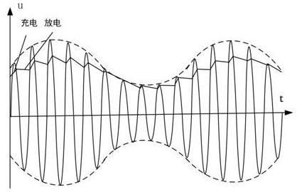
The invention discloses a graphene detector based on direct current bias. The graphene detector comprises a cavity, a signal input end, a signal output end and a graphene frequency multiplier substrate in the cavity, wherein the graphene frequency multiplier substrate comprises a high-frequency dielectric substrate and graphene arranged on the high-frequency dielectric substrate; the front end andthe rear end of the graphene are respectively connected to the signal input end and the signal output end through micro-strip lines; the front end of the graphene is connected to a direct current bias circuit and the rear end of the graphene is connected to an RC low pass filter; the direct current bias voltage loaded by the direct current bias circuit can be used for improving the detection effect of the graphene, and a baseband low-frequency signal is detected through a charge and discharge process of a capacitor and a resistor of the RC low-pass filter. The direct current bias is added, sothat the detection effect is improved. The design proves the feasibility of the graphene detector, and the graphene detector has the characteristics of being high in sensitivity, smaller in detectiondistortion, low in cost, simple in circuit and higher in working frequency.

Description

technical field [0001] The invention relates to a wave detector, in particular to a graphene wave detector and a design method based on a DC bias. Background technique [0002] Microwave detectors play an important role in systems such as communication, power detection, and test instruments. It is an essential device to ensure the normal operation of the millimeter wave system. From a functional point of view, the detector can demodulate the original modulation signal from the modulation signal without distortion, realize the shift of the spectrum, and transform the input high-frequency signal into the low-frequency signal at the output end. In recent years, due to its high electron mobility and good thermal conductivity, graphene is considered to be the next generation of electronic materials and has become a hot research direction. The detection circuit made of graphene has low efficiency and low reliability, and cannot be put into use. The design of the present inventio...

Claims


Application Information

Patent Timeline
Patent Type & Authority Patents(China)
IPC IPC(8): G01R19/00
CPCG01R19/00
Inventor 方勇盛浩轩侯学师陈敏梅寒郭勇钟晓玲
Owner CHENGDU UNIVERSITY OF TECHNOLOGY
Learn More