Infrared photoelectric detector and preparation method thereof

An electrical detector, infrared light technology, applied in circuits, electrical components, semiconductor devices, etc., can solve problems affecting the detection efficiency and detection limit of devices

Active Publication Date: 2014-03-26
PEKING UNIV
View PDF3 Cites 11 Cited by
  • Summary
  • Abstract
  • Description
  • Claims
  • Application Information

AI Technical Summary

Problems solved by technology

In any case, although the infrared detectors of carbon nanotubes have made some good progress, the small scale inhibits their excellent photoelectric performance, and it can be considered that the small diameter makes the interaction cross section with the detection light too small , which affects the detection efficiency and detection limit of the device, especially for weak infrared light [L.Y.Liu et al., Sensors and Actuators A116(2004)394]

Method used


Image

  • Infrared photoelectric detector and preparation method thereof
  • Infrared photoelectric detector and preparation method thereof
  • Infrared photoelectric detector and preparation method thereof

Examples


Embodiment 1

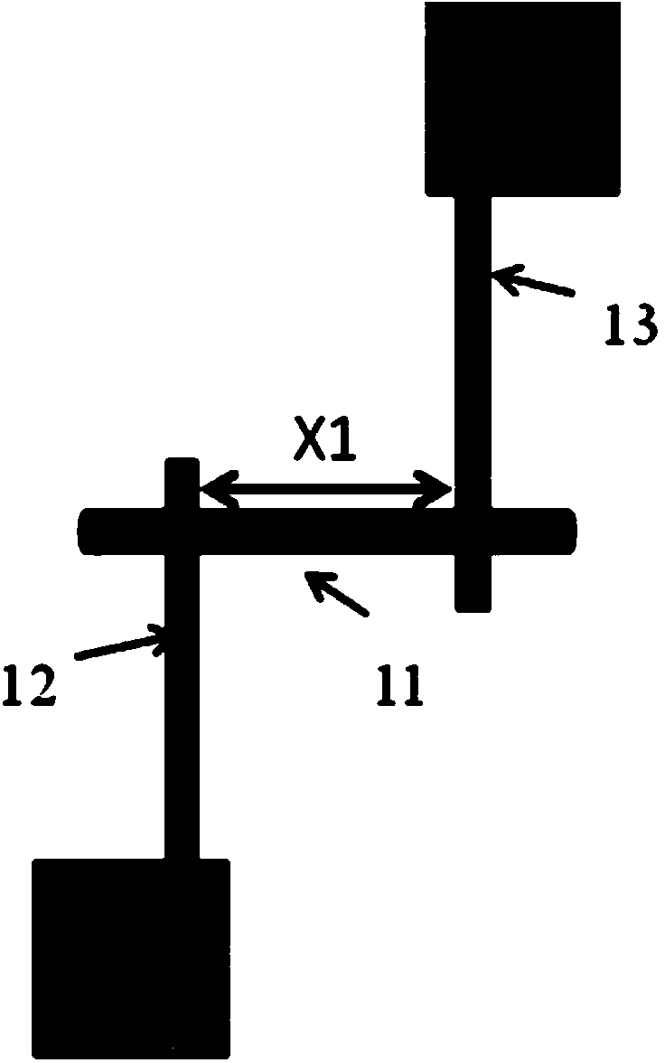
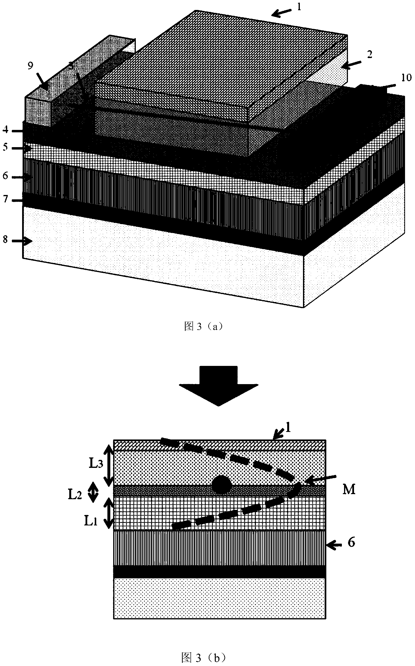
[0053] image 3 (a) shows the basic form of the infrared photodetector integrated semiconductor carbon nanotube diode and Fabry-Perot optical microcavity of the present invention. The semiconductor carbon nanotube 3 is entirely located on the hafnium oxide 4 substrate, and its two asymmetric electrodes are respectively between the palladium electrode 9 and the scandium electrode 10, with a distance of 1.5 microns. Wherein the electrode 9 is a palladium electrode with a width of about 1 micron, and the electrode 10 is a scandium (or yttrium) electrode with a width of about 1 micron. In the following example, we will illustrate the specific preparation steps for on-chip integration of the commonly used 1500 nm waveband, as follows:

[0054] 1. On the silicon substrates 7 & 8, an electron beam coater is used to deposit a silver reflective layer 6 of 130 nanometers and a silicon dioxide layer 5 of 165 nanometers respectively. Considering the easy oxidation of silver, the two are ...

Embodiment 2

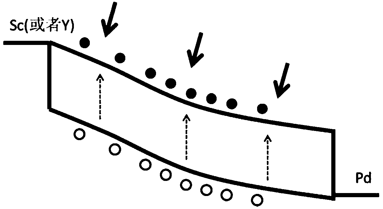
[0063] Image 6 It is based on the schematic diagram of the diode structure of multiple semiconducting carbon nanotubes. Figure 7 (a) Infrared photodetector integrated with semiconducting carbon nanotubes based on carbon nanotube film and Fabry-Perot optical microcavity shown in (a), the structural cross-sectional schematic diagram of the infrared photodetector is shown in Figure 7 (b) shown. The semiconducting carbon nanotube 3 is integrally located on the hafnium oxide 4 substrate, and its two asymmetric electrodes are respectively between the palladium electrode 9 and the yttrium electrode 21, with a difference X2 of 1 micron. Wherein the electrode 9 is a palladium electrode with a width of about 1.5 microns, and the electrode 21 is a yttrium electrode with a width of about 1.5 microns. In the following example, we will specifically describe the preparation of the on-chip integrated 1300nm waveband, as follows:

[0064] 1. On the silicon substrate 7 & 8, a 100-nm silve...


PUM


Abstract

The invention discloses an infrared photoelectric detector and a preparation method thereof. The detector comprises a substrate. An optical micro-cavity lower reflecting mirror, a lower optical path difference compensation layer, an upper optical path difference compensation layer and an optical micro-cavity upper reflecting mirror which are arranged on the substrate in turn. A semiconductor carbon nano-material photoelectric device used as a light absorption material and a conductive channel is arranged in an optical micro-cavity. The position of the optical micro-cavity with the maximum cavity state density is overlapped with a working area of the semiconductor carbon nano-material photoelectric device. As for infrared light with the same wavelength, an optical path through the lower optical path difference compensation layer is the same with the optical path through the upper optical path difference compensation layer, or difference of the two optical paths is integral times of half wavelength. Capability of detecting weak infrared light is enhanced, and the micro-cavity is simple and rapid in processing technology. The detector can be applied to interconnection of carbon tube circuit photoelectric devices or interconnection of carbon tubes and silicon integrated circuit sheets so that detection and response of communication wave band infrared light are executed.

Description

technical field [0001] The invention relates to an infrared light detector in the communication band, and relates to a photoelectric detector and a preparation method thereof, in particular to an infrared detector based on semiconductor carbon nanotubes and a preparation method thereof. Background technique [0002] Infrared photoelectric detection is a very important direction in the field of light detection, not only because of the importance of the infrared band to industry, military and science, including monitoring, manufacturing process control, biological and military infrared guidance and underwater exploration, etc. And it has become more important in the field of optical communication dominated by optical fiber and the increasingly important field of silicon-based optoelectronic integration. In the field of infrared detection, although traditional infrared detectors and materials have good performance, their preparation has bottlenecks such as harsh low-temperature...

Claims


Application Information

Patent Timeline
Patent Type & Authority Applications(China)
IPC IPC(8): H01L31/0232H01L31/101H01L31/18
CPCH01L31/02327H01L31/101Y02P70/50
Inventor 梁爽王胜魏楠彭练矛
Owner PEKING UNIV
Why Eureka
Try Eureka