Multi-quantum well structure, and LED epitaxial wafer and preparation method thereof

A technology of multi-quantum well structure and LED epitaxial wafer, which is applied in the direction of electrical components, circuits, semiconductor devices, etc., and can solve the problems of reducing internal quantum efficiency and other issues

Inactive Publication Date: 2019-10-15
SHANDONG INSPUR HUAGUANG OPTOELECTRONICS
View PDF11 Cites 2 Cited by
  • Summary
  • Abstract
  • Description
  • Claims
  • Application Information

AI Technical Summary

Problems solved by technology

After the current is injected, the electrons in the n-type GaN layer will easily pass through the light-emitting layer (active layer MQW) due to their high mobility,

Method used


Image

  • Multi-quantum well structure, and LED epitaxial wafer and preparation method thereof
  • Multi-quantum well structure, and LED epitaxial wafer and preparation method thereof
  • Multi-quantum well structure, and LED epitaxial wafer and preparation method thereof

Examples


Embodiment 1

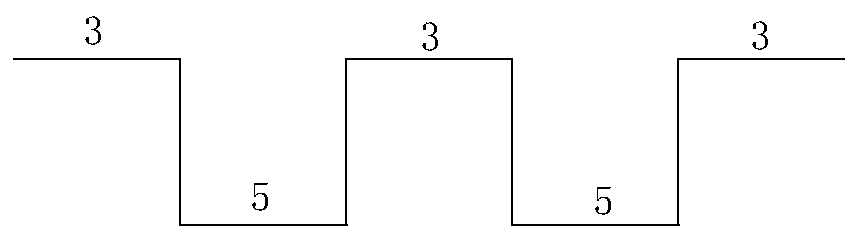
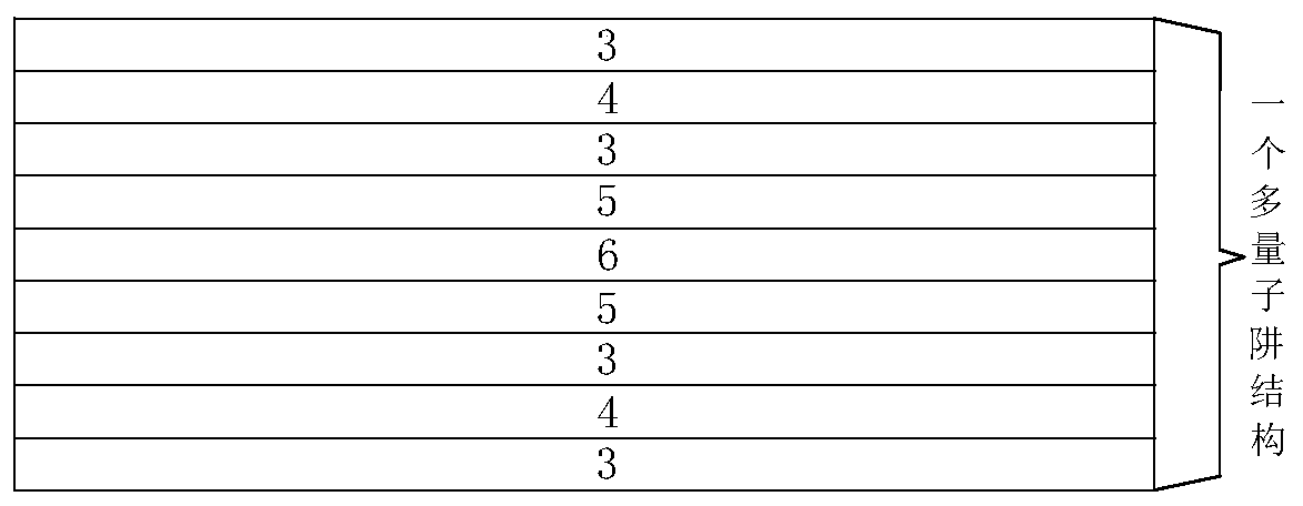
[0044] Embodiment 1, a multi-quantum well structure, is a 9-layer upper and lower layer superposition structure, and the 9 layers are grown sequentially from bottom to top;

[0045] The first layer is GaN barrier layer 3, the second layer is AlGaN barrier layer 4, the third layer is GaN barrier layer 3, the fourth layer is InGaN potential well layer 5, and the fifth layer is low-temperature InGaN potential well layer 6 , the sixth layer is an InGaN potential well layer 5, the seventh layer is a GaN barrier layer 3, the eighth layer is an AlGaN barrier layer 4, and the ninth layer is a GaN barrier layer 3;

[0046] The first layer, the second layer, the third layer, the fourth layer, the fifth layer, the sixth layer, the seventh layer, the eighth layer, and the ninth layer are stacked in order from bottom to top.

Embodiment 2

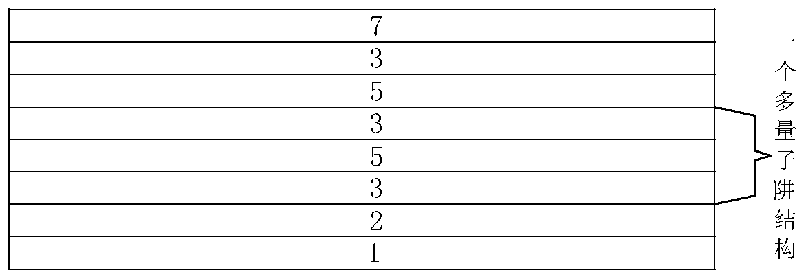
[0047] Embodiment 2, an LED epitaxial wafer, including a substrate 1, an N-type layer 2, 5-9 multi-quantum well structures and a P-type layer 7, each of the 5-9 multi-quantum well structures Both are the multi-quantum well structure in the above-mentioned embodiment 1;

[0048] 5 to 9 multi-quantum well structures are stacked sequentially from bottom to top;

[0049] The substrate 1 , N-type layer 2 , 5-9 multi-quantum well structures, and P-type layer 7 are stacked and arranged sequentially from bottom to top.

Embodiment 3

[0050] Embodiment 3, a method for preparing the above-mentioned LED epitaxial wafer, comprising the following steps in sequence:

[0051] 1) growing an N-type layer 2 structure on the substrate 1;

[0052] 2) growing a multi-quantum well structure on the upper surface of the N-type layer 2;

[0053] The preparation method of the multiple quantum well structure comprises the following steps carried out in sequence:

[0054] a) growing a first layer on the upper surface of the N-type layer 2, the first layer being a GaN barrier layer 3;

[0055] b) growing a second layer on the upper surface of the first layer, the second layer being an AlGaN barrier layer 4;

[0056] c) growing a third layer on the upper surface of the second layer, the third layer being a GaN barrier layer 3;

[0057] d) growing a fourth layer on the upper surface of the third layer, the fourth layer being an InGaN potential well layer 5;

[0058] e) growing a fifth layer on the upper surface of the fourth...


PUM

PropertyMeasurementUnit
Thicknessaaaaaaaaaa

Abstract

The invention provides a multi-quantum well structure. The multi-quantum well structure is a structure formed by stacking nine layers up and down, wherein the nine layers comprises in order from bottom to top: a GaN barrier layer, an AlGaN barrier layer, a GaN barrier layer, an InGaN potential well layer, a low-temperature InGaN potential well layer, an InGaN potential well layer, a GaN barrier layer, an AlGaN barrier layer and a GaN barrier layer. The invention also provides an LED epitaxial wafer. The invention also provides a preparation method of the LED epitaxial wafer. The method can effectively reduce the stress between well and barrier interfaces and can relieve the bending of energy bands, the AlGaN barrier layer can effectively strengthen the blocking of electrons, and the low-temperature InGaN potential well layer can improve the efficiency of injecting holes and electrons into the active area and the radiation recombination efficiency, thereby fundamentally improving the crystal quality and the internal quantum efficiency, further improving the performance of devices and improving the light extraction efficiency of the active area by about 37%.

Description

technical field [0001] The invention relates to the technical field of LED epitaxial design, in particular to a multi-quantum well structure, an LED epitaxial wafer and a preparation method thereof. Background technique [0002] In the early 1990s, the third-generation wide-bandgap semiconductor materials represented by nitrides made a historic breakthrough. Researchers successfully prepared blue-green and ultraviolet LEDs on gallium nitride materials, making LED lighting become possible. In 1971, the first gallium nitride LED die came out. In 1994, gallium nitride HEMTs appeared blue light GaN-based diodes with high electron mobility, and gallium nitride semiconductor materials developed very rapidly. [0003] Semiconductor light-emitting diodes have the advantages of small size, ruggedness, strong controllability of light-emitting bands, high luminous efficiency, low heat loss, low light decay, energy saving, and environmental protection. Communication and other fields h...

Claims


Application Information

Patent Timeline
IPC IPC(8): H01L33/00H01L33/06H01L33/14
CPCH01L33/007H01L33/06H01L33/14H01L33/145
Inventor 柳颜欣马旺王成新
Owner SHANDONG INSPUR HUAGUANG OPTOELECTRONICS
Why Eureka
Try Eureka