Secondary via hole reflow soldering method

A secondary via and reflow soldering technology, which is applied in the manufacture of printed circuits, electrical components, printed circuits, etc., to achieve the effects of improving PCB solderability, shortening production cycle, and reducing materials and personnel

Inactive Publication Date: 2019-10-18
SHENZHEN HHY ELECTRONICS TECH CO LTD
View PDF2 Cites 1 Cited by
  • Summary
  • Abstract
  • Description
  • Claims
  • Application Information

AI Technical Summary

Problems solved by technology

[0004] The present invention proposes a secondary via-hole reflow soldering method, PIHR via-hole reflow soldering technology (Pin-In-HoleReflow, referred to as PIHR), which effectively improves the deficiencies of the wave soldering process, improves the PCB yield, and avoids false soldering, Reduce the defect rate such as missing soldering, reduce environmental pollution and other problems

Method used


Image

  • Secondary via hole reflow soldering method

Examples


Embodiment Construction

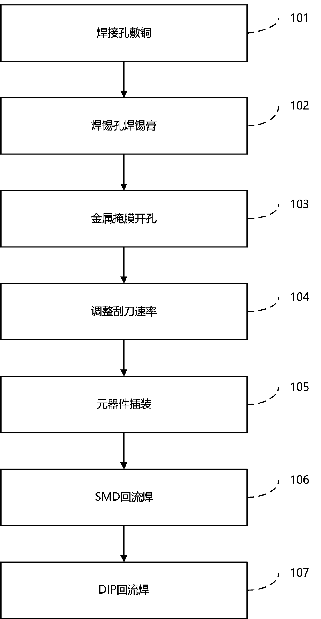
[0024] The present invention will be described in further detail below in conjunction with the embodiments and the accompanying drawings, but the embodiments of the present invention are not limited thereto.

[0025] At present, due to the thickness of some PCBs in the via reflow soldering process is 1.6T, and the pins of some components are hollow, after the reflow soldering process, the non-component surface of the PBA shows that the amount of tin is insufficient. In fact, the inside has been soldered. Some technologies use partially thickened aluminum alloy steel mesh (Mental Mask) to solve it.

[0026] For the via-hole reflow soldering process, the soldering state of the solder joint depends on the volume of the alloy formed after the reflow of the solder in the solder hole. Since the volume of the solder paste is reduced to about 50% of the tin content, for thicker PCB through holes Due to the reduction of the attachment carrier of the solder paste, it is more likely to h...


PUM

PropertyMeasurementUnit
areaaaaaaaaaaa
areaaaaaaaaaaa
thicknessaaaaaaaaaa

Abstract

The invention provides a secondary via hole reflow soldering method. According to the technical schemes of the invention, copper is applied to the surfaces of soldering tin holes needing to be welded,so that the excellent copper application of the soldering tin holes can be realized; the positions of the soldering tin holes are printed with soldering paste; aluminum alloy steel mesh trepanning isperformed on a PCB, so that the soldering tin holes can be completely covered; the speed of a scraper is adjusted, so that the soldering paste is applied to and fully fills the soldering tin holes; components are inserted into the soldering tin holes; and welding is carried out through secondary via hole reflow soldering, at first, SMD (Surface Mounted Device) reflow soldering is carried out, andthen DIP (Dual In-line Package) reflow soldering is carried out. With the via hole reflow soldering method of the invention adopted, the defects of a wave soldering process are effectively eliminated; the yield of the PCB is improved; reject ratios caused by insufficient welding and missed welding are avoided; and the problems of environmental pollution and the like are reduced.

Description

technical field [0001] The invention relates to the technical field of soldering of electronic products, in particular to a secondary via hole reflow soldering process of a circuit board. Background technique [0002] In the traditional electronic assembly process, wave soldering technology is generally used for soldering PCB (PCBA, Printed Circuit Board, printed circuit board) with through-hole components installed, but wave soldering has many shortcomings: 1. Not suitable for small Welding of chemical, multi-functional, high-density, and fine-pitch components, the welding accuracy cannot meet the requirements of precision electronic products; 2. There are many bridging and missing soldering; 3. Flux needs to be sprayed during the welding process, and there are volatile substances in the flux , such as alcohol, pollutes the environment; 4. The printed board is warped and deformed by a large thermal shock. Therefore, wave soldering cannot adapt to the development of electro...

Claims


Application Information

Patent Timeline
Patent Type & Authority Applications(China)
IPC IPC(8): H05K3/34
CPCH05K3/3494H05K2203/043
Inventor 马克俊
Owner SHENZHEN HHY ELECTRONICS TECH CO LTD
Why Eureka
Try Eureka