
Semiconductor process equipment and method for manufacturing semiconductor device

A process equipment and semiconductor technology, applied in semiconductor/solid-state device manufacturing, electrical components, circuits, etc., can solve problems such as affecting yield, failing to meet device design specifications, and poor thickness uniformity

Active Publication Date: 2021-04-09
SEMICON MFG INT (SHANGHAI) CORP +1
View PDF7 Cites 0 Cited by
  • Summary
  • Abstract
  • Description
  • Claims
  • Application Information

AI Technical Summary

Problems solved by technology

The quality of epitaxial layer growth (including thickness, thickness uniformity, doping concentration, etc.) is crucial to the performance of the device, but the thickness uniformity of the epitaxial layer grown by the current epitaxial growth equipment is poor, which cannot meet the design specifications of the device. and affect yield

Method used


Image

  • Semiconductor process equipment and method for manufacturing semiconductor device
  • Semiconductor process equipment and method for manufacturing semiconductor device
  • Semiconductor process equipment and method for manufacturing semiconductor device

Examples


Embodiment Construction

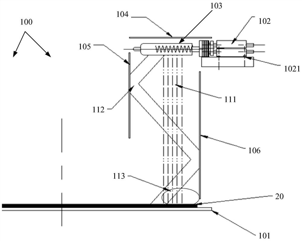
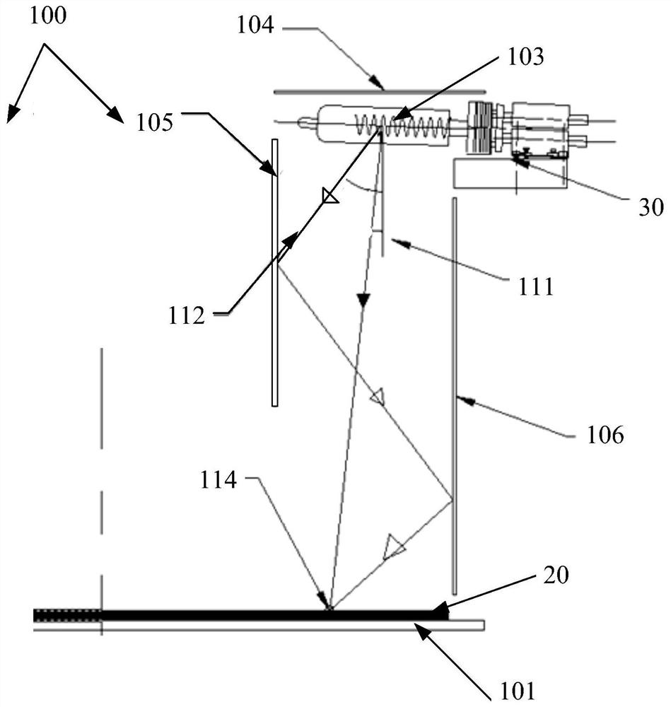
[0031] Silicon germanium (SiGe) is an important semiconductor material after silicon and gallium arsenide. It has better characteristics than pure silicon and is compatible with silicon in process. At the same time, the cost of silicon germanium is lower than that of gallium arsenide. , but the performance of devices and circuits made of silicon germanium can almost reach the level of compound semiconductor devices and circuits such as gallium arsenide. Therefore, silicon germanium technology has become an important direction for the development of microelectronics technology, and in many devices In the manufacturing process of the silicon germanium film layer, it needs to be realized by the epitaxial growth process. A commonly used epitaxial growth equipment for epitaxial growth of SiGe film, such as Figure 1A As shown, it includes a reaction chamber 100, a wafer carrying base 101, a fixed lamp socket (lamp sockets) 102, a heating lamp group (outer lamp & inner lamp) 103, a r...


PUM


Abstract

The invention provides a semiconductor process equipment and a manufacturing method of a semiconductor device. In the semiconductor process equipment, the fixed lamp holder is changed into an adjustable lamp holder, so that the incident angle of the emitted light of the heating lamp group can be adjusted, and then the heating cover can be adjusted. The reflected light reflected by the group and the direct light directly emitted by the heating lamp group are both focused on the same position on the wafer surface, avoiding the cold area caused by the crossing of the reflected light and the direct light, thereby improving the thickness uniformity of the formed film layer to meet the requirements of the device. manufacturing requirements. In the manufacturing method of the semiconductor device, the semiconductor process equipment is used to manufacture the required film layer, which can improve the thickness uniformity of the formed film layer and improve the device yield.

Description

technical field [0001] The invention relates to the technical field of integrated circuit manufacturing, in particular to a semiconductor process equipment and a semiconductor device manufacturing method. Background technique [0002] Epitaxy (Epitaxy, referred to as Epi) process refers to growing a single crystal material with the same lattice arrangement as the single crystal substrate on a single crystal substrate, and the epitaxial layer can be a homoepitaxial layer (such as silicon Si / Si ), or a heteroepitaxial layer (such as silicon germanium SiGe / Si or silicon carbon SiC / Si, etc.). The quality of epitaxial layer growth (including thickness, thickness uniformity, doping concentration, etc.) is crucial to the performance of the device, but the thickness uniformity of the epitaxial layer grown by the current epitaxial growth equipment is poor, which cannot meet the design specifications of the device. And affect the yield. Contents of the invention [0003] The objec...

Claims


Application Information

Patent Timeline
Patent Type & Authority Patents(China)
IPC IPC(8): H01L21/67
CPCH01L21/67115
Inventor 杨维军马彪黄凌燕
Owner SEMICON MFG INT (SHANGHAI) CORP
Learn More