GaN-based semiconductor light emitting device having AlGaN interposer and manufacturing method thereof

A technology of light-emitting devices and manufacturing methods, which is applied to semiconductor lasers, laser components, lasers, etc., can solve problems such as increased current leakage, reduced luminous uniformity, and uneven quantum well/barrier interfaces, so as to improve luminous uniformity, The effect of increasing the steepness of the interface and eliminating V-shaped defects

Inactive Publication Date: 2019-11-01
SUZHOU INST OF NANO TECH & NANO BIONICS CHINESE ACEDEMY OF SCI
View PDF4 Cites 3 Cited by
  • Summary
  • Abstract
  • Description
  • Claims
  • Application Information

AI Technical Summary

Problems solved by technology

[0003] Due to the low suitable growth temperature of indium gallium nitride materials, gallium nitride quantum barriers can only be grown at relatively low temperatures. The resulting V-shaped defects and interface fluctuations will cause the quantum well / barrier interface to be uneven and increase the current. Leakage, reduced luminous uniformity
[0004] For example, in GaN-based lasers, the unevenness of the interface can cause problems such as broadening of the gain spectrum, increased threshold current, and decreased slope efficiency
At present, the current gallium nitride-based optoelectronic devices generally have such problems, which seriously affect the luminous effect

Method used


Image

  • GaN-based semiconductor light emitting device having AlGaN interposer and manufacturing method thereof
  • GaN-based semiconductor light emitting device having AlGaN interposer and manufacturing method thereof
  • GaN-based semiconductor light emitting device having AlGaN interposer and manufacturing method thereof

Examples


Embodiment Construction

[0029] In order to make the object, technical solution and advantages of the present invention more clear, the present invention will be further described in detail below in conjunction with the accompanying drawings and embodiments. It should be understood that the specific embodiments described here are only used to explain the present invention, not to limit the present invention.

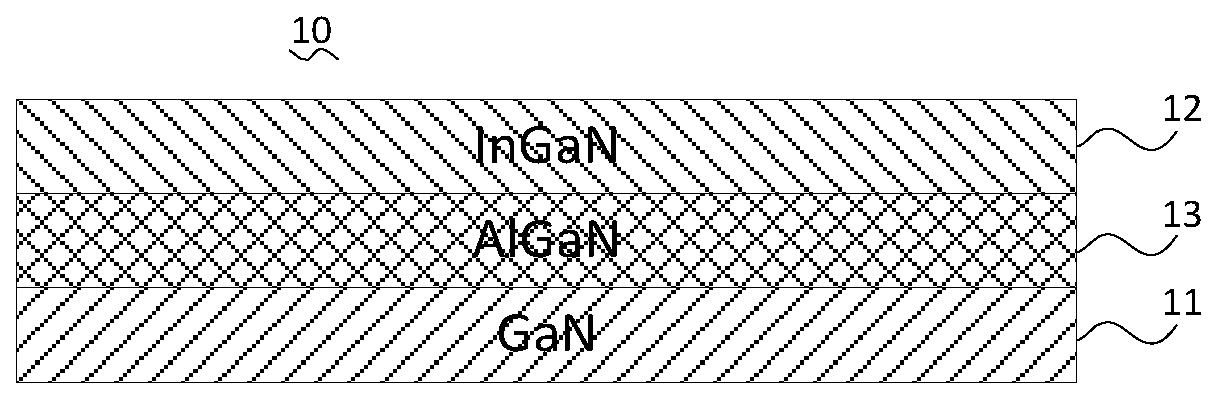
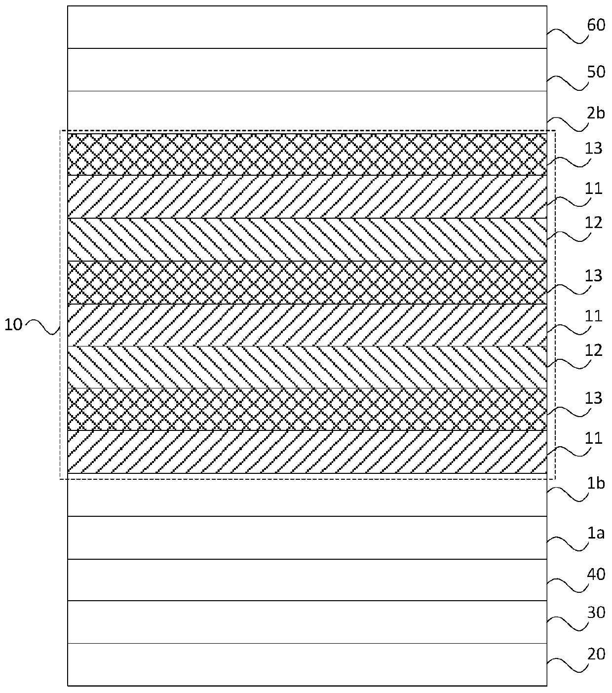
[0030] refer to figure 1 , the quantum well structure 10 of the embodiment of the present invention includes at least one set of gallium nitride (GaN) quantum barriers 11 and indium gallium nitride (InGaN) quantum wells 12, each set of gallium nitride quantum barriers 11 and indium gallium nitrogen quantum wells 12 There is at least one aluminum gallium nitride (AlGaN) insertion layer 13 between them. That is, after the growth of the GaN quantum barrier 11 is completed and before the growth of the InGaN quantum well 12, at least one insertion layer of AlGaN material is inserted, and the AlGaN i...


PUM


Abstract

The invention discloses a GaN-based semiconductor light emitting device having an AlGaN interposer and a manufacturing method thereof. The semiconductor light emitting device includes a quantum well structure, wherein the quantum well structure includes at least one set of gallium nitride quantum barriers and indium gallium nitride quantum wells, and each set of gallium nitride quantum barriers and indium gallium nitride quantum wells includes at least a layer of aluminum gallium nitride insertion layer. The semiconductor light emitting device is advantaged in that the aluminum gallium nitrideinsertion layer is utilized between the gallium nitride quantum barriers and the indium gallium nitride quantum wells of the quantum well structure, obtaining atomic level flat surfaces on the gallium nitride quantum barriers, improving interface steepness and eliminating V-shaped defects are not only facilitated, device leakage is reduced, light emitting uniformity is improved, but also balancing the stress accumulated during growth of the indium gallium nitride quantum wells is further facilitated, dislocation of quantum well materials due to accumulation of strain energy is reduced, and thereby improvement of the quality of material forming is facilitated.

Description

technical field [0001] The invention relates to the technical field of semiconductor devices, in particular to the field of gallium nitride (GaN) optoelectronic devices, and relates to a gallium nitride-based semiconductor light-emitting device with an aluminum gallium nitride (AlGaN) insertion layer and a manufacturing method thereof. Background technique [0002] GaN-based optoelectronic devices have been widely used in lighting, display and other fields. As the active region of the visible light device, InGaN / GaN MQW is the core of the whole device. [0003] Due to the low suitable growth temperature of indium gallium nitride materials, gallium nitride quantum barriers can only be grown at relatively low temperatures. The resulting V-shaped defects and interface fluctuations will cause the quantum well / barrier interface to be uneven and increase the current. Leakage, reduced uniformity of light emission. [0004] For example, in GaN-based lasers, the unevenness of the i...

Claims


Application Information

Patent Timeline
Patent Type & Authority Applications(China)
IPC IPC(8): H01S5/343
CPCH01S5/34333
Inventor 张峰池田昌夫刘建平张书明李德尧张立群杨辉
Owner SUZHOU INST OF NANO TECH & NANO BIONICS CHINESE ACEDEMY OF SCI
Why Eureka
Try Eureka