

Preparation method of area thick film silicon nitride
A thick-film silicon nitride and area technology, which is applied in the field of integrated optics, can solve problems such as difficult large-area growth, CMP inhomogeneity, and poor device sidewall steepness, and solve the problems that are not conducive to the preparation of highly integrated waveguides. device, beneficial to highly integrated, thick film growth effect
- Summary
- Abstract
- Description
- Claims
- Application Information
AI Technical Summary
Problems solved by technology
Method used
Image


Examples
preparation example Construction
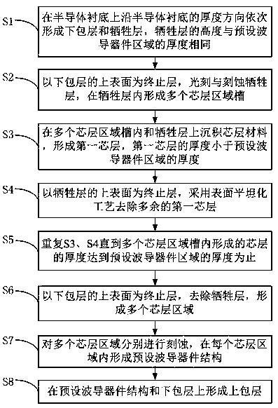
[0027] In this embodiment, a method for preparing a regional thick film silicon nitride, such as figure 1 shown, including:
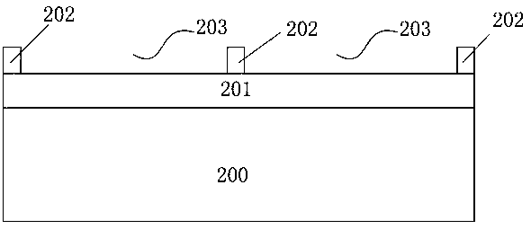
[0028] S1, sequentially forming a lower cladding layer and a sacrificial layer on the semiconductor substrate along the thickness direction of the semiconductor substrate, and the height of the sacrificial layer is the same as the thickness of the predetermined waveguide device region;
[0029] On the basis of the above solutions, further, the semiconductor substrate in this implementation manner is a silicon substrate, and in other implementation manners, the semiconductor substrate may also be a quartz substrate.
[0030] On the basis of the above solution, further, the lower cladding layer is formed by thermal oxidation and / or chemical vapor deposition process, and in other embodiments, the lower cladding layer can also be formed by physical vapor deposition process. The lower cladding material includes a solid cladding material with a refractive in...
PUM
| Property | Measurement | Unit |
|---|---|---|
| Thickness | aaaaa | aaaaa |
| Thickness | aaaaa | aaaaa |
Abstract
Description
Claims
Application Information