Process for producing integrated circuit, and substrate with integrated circuit

a technology of integrated circuits and substrates, applied in the direction of mechanical vibration separation, superimposed coating process, liquid/solution decomposition chemical coating, etc., to achieve the effects of low wiring resistance, high density, and high degree of integration

Inactive Publication Date: 2007-01-16
JGC CATALYSTS & CHEM LTD
View PDF14 Cites 1 Cited by
  • Summary
  • Abstract
  • Description
  • Claims
  • Application Information

AI Technical Summary

Benefits of technology

[0010]The present invention has been made with a view toward solving the above problems of the prior art. Therefore, it is an object of the present invention to provide a process for producing an integrated circuit, wherein not only can conductive fine particles be deposited efficiently and densely in minute wiring channels ...

Problems solved by technology

Furthermore, the vibrational energy of ultrasonic waves is transmitted to conductive fine particles, so that the conductive fine part...

Method used


Image

  • Process for producing integrated circuit, and substrate with integrated circuit
  • Process for producing integrated circuit, and substrate with integrated circuit
  • Process for producing integrated circuit, and substrate with integrated circuit

Examples


example

[0111]The present invention will further be illustrated below with reference to the following Examples which in no way limit the scope of the invention.

preparation example

Preparation of Dispersion of Conductive Fine Particles

[0112]The compositions of dispersions of metal fine particles and conductive fine particles used in the Examples and Comparative Examples are specified in Table 1.

[0113]Dispersions of metal fine particles (Q-1, Q-2 and Q-3) were prepared in the following manner.

[0114]First, trisodium citrate was added to 100 g of pure water in an amount corresponding to 0.01 part by weight per part by weight of metal fine particles. Aqueous solutions of silver nitrate, palladium nitrate and copper chloride were added thereto so that the concentration in terms of metal was 10% by weight and so that the metal species had weight ratios specified in Table 1. Further, an aqueous solution of ferrous sulfate was added in a molar amount equal to the total mole of silver nitrate, palladium nitrate and copper chloride and agitated for 1 hr in an atmosphere of nitrogen. Thus, dispersions of metal fine particles were obtained. The resultant dispersions were ...

example 1

[Formation of Substrate with Integrated Circuit]

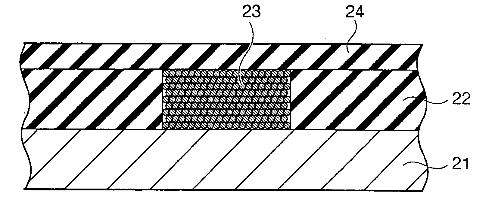
[0123]A substrate of silicon wafer (8-inch wafer) sequentially overlaid with insulating films, namely, insulating film A of silicon nitride (thickness: 0.2 μm), insulating film B of silica (thickness: 0.4 μm) superimposed on a surface of insulating film A and insulating film C of silicon nitride (thickness: 0.2 μm) superimposed on a surface of insulating film B was coated with a positive photoresist, and subjected to a 0.3 μm line-and-space exposure.

[0124]Subsequently, the exposed portions were removed with the use of a developer containing tetramethylammonium hydride (TMAH). Under layer insulating films were patterned with the use of a mixture of CF4 and CHF3 gases. The remaining resist was removed by irradiating the same with O2 plasma. Thus, wiring channels having a width (Wc) of 0.3 μm, a depth (Dc) of 0.6 μm and an aspect ratio (Dc / Wc) of 2 were formed.

[0125]Separately, the above prepared dispersion for integrated circuit formatio...


PUM

PropertyMeasurementUnit
Fractionaaaaaaaaaa
Percent by massaaaaaaaaaa

Abstract

There is provided a process for producing an integrated circuit, wherein not only can conductive fine particles be deposited efficiently and densely in minute wiring channels and connecting holes but also a circuit of low wiring resistance and high density can be formed and wherein a high-degree integration can be achieved to thereby bring about an economic advantage. In particular, there is provided a process for producing an integrated circuit, comprising coating a substrate provided with wiring channels with a coating liquid for integrated circuit formation containing conductive fine particles to thereby form an integrated circuit on the substrate, wherein the coating liquid for integrated circuit formation while being exposed to ultrasonic waves is applied to the wiring channels.

Description

BACKGROUND OF THE INVENTION[0001]1. Field of the Invention[0002]The present invention relates to a process for producing an integrated circuit, including coating a substrate provided with wiring channels with a coating liquid for integrated circuit formation containing a component for conductive fine particle formation and / or conductive fine particles to thereby form an electrical circuit on the substrate, wherein the coating liquid for integrated circuit formation while being exposed to ultrasonic waves is applied to the wiring channels. The present invention also relates to a substrate with integrated circuit produced by this process.[0003]2. Description of the Prior Art[0004]Various integrated circuits are used in computers and other various electronic equipments. An increase of circuit density and an enhancement of circuit performance are demanded in accordance with the trend toward miniaturization and sophistication of such equipments.[0005]In particular, for example, semicondu...

Claims


Application Information

Patent Timeline
IPC IPC(8): H01L21/44H01L21/336H01L21/4763H01L21/288H01L21/768
CPCH01L21/76877H01L21/288H01L21/3205
Inventor TONAI, ATSUSHIHIRAI, TOSHIHARUKOYANAGI, TSUGUOMATSUDA, MASAYUKIKOMATSU, MICHIO
Owner JGC CATALYSTS & CHEM LTD
Why Eureka
Try Eureka