Film layer structure, manufacturing method thereof and filter comprising film layer structure

A technology of film layer structure and manufacturing method, applied in electrical components, impedance networks, etc., can solve problems such as the decrease of effective electromechanical coupling coefficient, the deterioration of the preferred orientation of piezoelectric materials, and the influence of filter insertion loss, so as to reduce device insertion loss. and the effect of bandwidth, improving device temperature stability, reducing the effect of performance

Pending Publication Date: 2019-11-15
CHINA ELECTRONICS TECH GRP NO 26 RES INST
View PDF6 Cites 11 Cited by
  • Summary
  • Abstract
  • Description
  • Claims
  • Application Information

AI Technical Summary

Problems solved by technology

However, this approach is not feasible in practical applications
In 2008, Brice Ivira added SiO to the piezoelectric reactor 2 to achieve temperature compensation, but SiO 2 The lattice does not match with the piezoelectric material, and the stress is not easy to control, which will lead to the deterioration of the preferred ...

Method used


Image

  • Film layer structure, manufacturing method thereof and filter comprising film layer structure
  • Film layer structure, manufacturing method thereof and filter comprising film layer structure
  • Film layer structure, manufacturing method thereof and filter comprising film layer structure

Examples


Embodiment Construction

[0033] In order to make the purpose, technical solutions and advantages of the present invention clearer, the technical solutions in the embodiments of the present invention will be clearly and completely described below in conjunction with the accompanying drawings. Obviously, the described embodiments are only part of the embodiments of the present invention, and Not all examples.

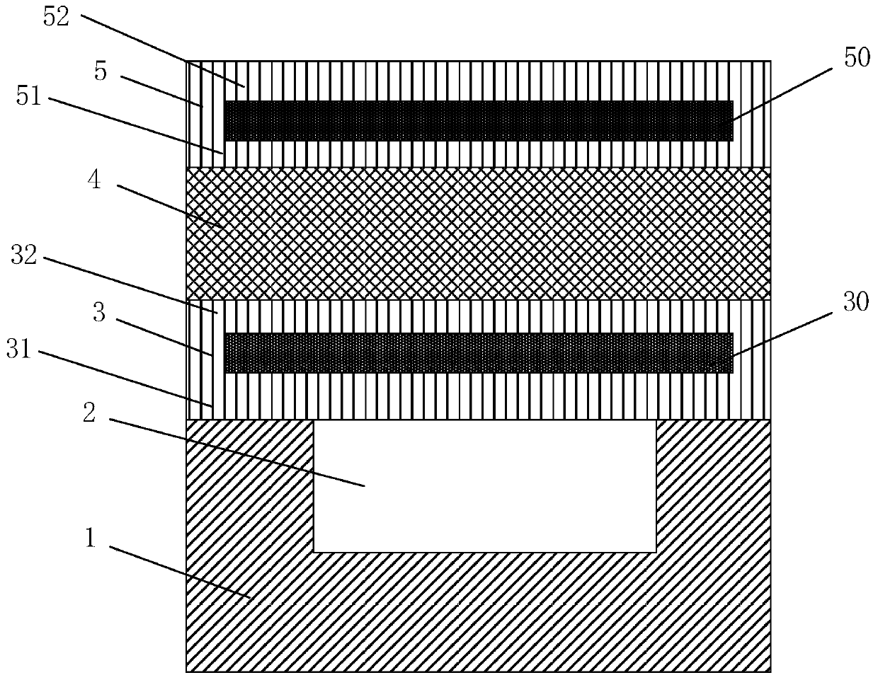
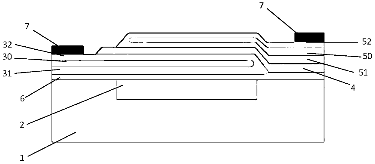
[0034] Such as figure 1 As shown, a film layer structure of the present invention includes a substrate 1, a cavity 2 is opened on the top of the substrate 1, and a composite upper electrode 5 and a composite lower electrode 3 are prepared above the substrate 1. , a piezoelectric layer 4 is arranged between the composite upper and lower electrodes, and the composite upper electrode 5 includes an upper electrode 52, a first temperature compensation layer 50 and an upper electrode insertion layer 51 arranged from top to bottom; the composite The lower electrode includes a lower electrode insertion ...


PUM

PropertyMeasurementUnit
Thicknessaaaaaaaaaa
Thicknessaaaaaaaaaa
Thicknessaaaaaaaaaa

Abstract

The invention belongs to the technical field of film bulk acoustic wave filter processes, and particularly provides a film layer structure, a manufacturing method thereof and a filter comprising the film layer structure. The film layer structure comprises a substrate, a cavity is formed in the top of the substrate, a composite upper electrode and a composite lower electrode are prepared above thesubstrate, and a piezoelectric layer is arranged between the composite upper electrode and the composite lower electrode; wherein the composite upper electrode comprises an upper electrode, a first temperature compensation layer and an upper electrode insertion layer which are arranged from top to bottom; and the composite lower electrode comprises a lower electrode insertion layer, a second temperature compensation layer and a lower electrode which are arranged from top to bottom. Through the film layer structure provided by the invention, the C-axis preferred orientation growth of the piezoelectric film is facilitated, the piezoelectric film with good orientation and complete crystal grain growth is obtained, and in addition, a filter adopting the film layer structure can be ensured to have relatively low insertion loss and keep bandwidth stable.

Description

technical field [0001] The invention relates to a film layer structure and technology of a high-temperature-stable thin-film bulk acoustic wave filter (TC-FBAR), and belongs to the technical field of thin-film bulk acoustic wave filter technology. Background technique [0002] With the continuous improvement of the operating frequency, sensitivity and integration of military electronic equipment, phased array radar, electronic countermeasures and communication systems have put forward an urgent need for filters with frequency temperature coefficient, high performance and small size. Thin film bulk acoustic wave filter is used in the RF front-end to isolate and gate the RF signal, limit the radiation signal of the transmitter in its operating frequency band, and prevent the interference of the received noise signal. It is a key device in the RF system. It plays a vital role in the competition for control of electromagnetic power. At present, the frequency temperature coeffic...

Claims


Application Information

Patent Timeline
IPC IPC(8): H03H3/04H03H3/02
CPCH03H3/04H03H3/02H03H2003/023H03H2003/0407H03H2003/0414
Inventor 刘娅马晋毅徐阳蒋平英田本郎杨正兵谭发曾梁柳红唐小龙兰伟豪
Owner CHINA ELECTRONICS TECH GRP NO 26 RES INST
Why Eureka
Try Eureka