
High-frequency high-speed and high-density circuit board manufacturing process

A circuit board manufacturing, high-density technology, applied in the direction of printed circuit manufacturing, printed circuit, printed circuit, etc., can solve the problems of external energy consumption, difficulty, external energy waste, etc., to improve the air circulation speed and improve the stability of use , Increase the effect of cooling speed

Inactive Publication Date: 2019-11-15
四川深北电路科技有限公司
View PDF7 Cites 0 Cited by
  • Summary
  • Abstract
  • Description
  • Claims
  • Application Information

AI Technical Summary

Problems solved by technology

[0005] The purpose of the present invention is to provide a high-frequency, high-speed, high-density circuit board manufacturing process to solve the problem that the existing circuit boards proposed in the above background technology will accumulate heat under the requirements of high-frequency, high-speed, and high-density use, which cannot be effectively processed. The rapid heat dissipation of the circuit board affects the accuracy and life of the circuit board. It needs to cooperate with the external heat dissipation device, which results in the consumption of external energy. In the external heat dissipation process of the circuit board in the face of large volume, large range and special environment In the process, it will cause huge waste of external energy and difficult disadvantages

Method used


Image

  • High-frequency high-speed and high-density circuit board manufacturing process
  • High-frequency high-speed and high-density circuit board manufacturing process
  • High-frequency high-speed and high-density circuit board manufacturing process

Examples


Embodiment

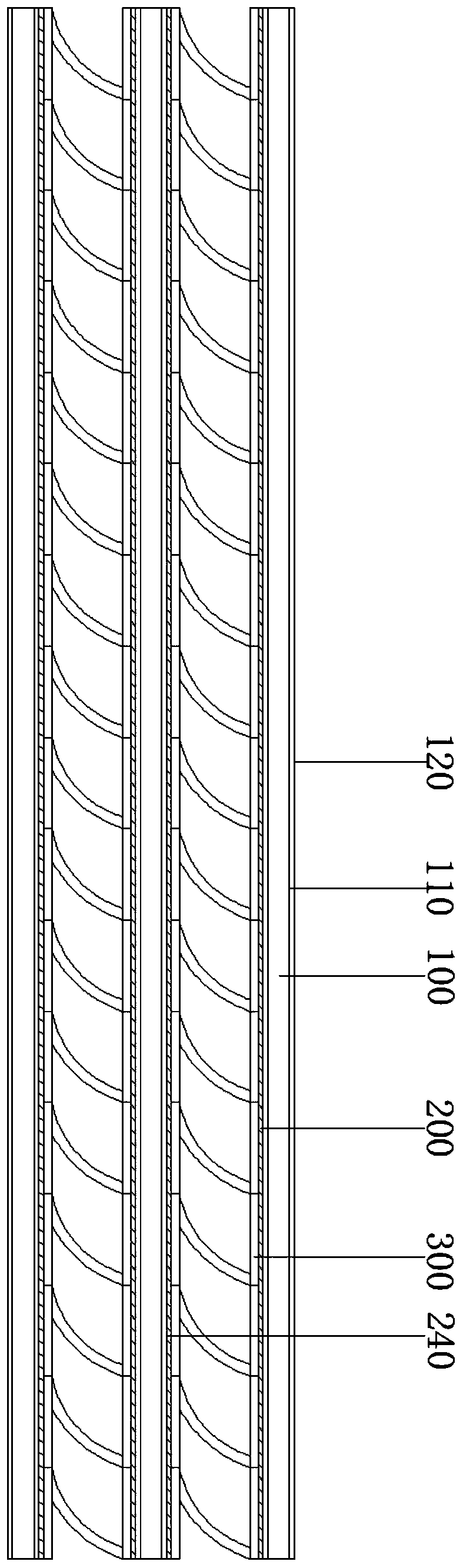
[0043] S1: select the double-sided copper plate 100 to cut into workpieces of different sizes according to the needs of production, and select the predetermined workpiece size according to the size, so as to avoid waste and increase unnecessary costs;

[0044] S2: Copper foil 120 is processed, before being combined with the outer layer, copper foil 120 will be oxidized to form a fine concave-convex surface, and the oxidation treatment time is 35min;

[0045]S3: Paste the photosensitive dry film on the double-sided copper plate 100 as the inner layer, then stick to the film used to make the inner layer wiring, expose, and then perform imaging processing, leaving only the wiring required place, remove unnecessary copper foil 120 by etching;

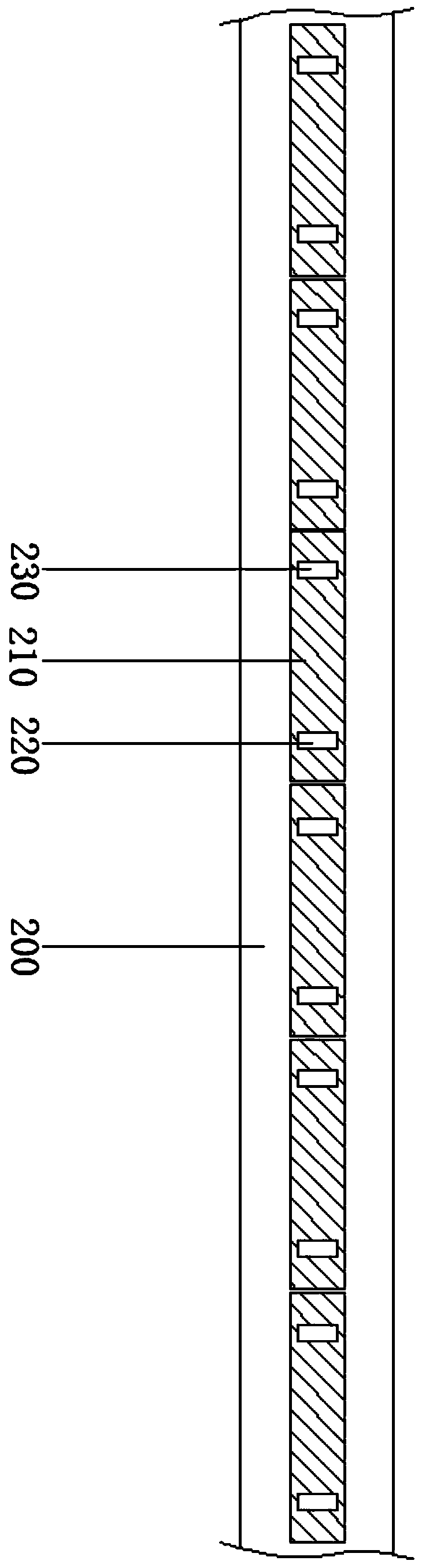
[0046] S4: the oxidized double-sided copper plate 100 and the outer combined outer layer copper plate 110 are heated in a vacuum state while being compressed by a laminator, and the pressure is normal pressure to form a circuit unit;

[00...


PUM


Abstract

The invention belongs to the technical field of manufacturing processes, and particularly relates to a high-frequency high-speed and high-density circuit board manufacturing process. The high-frequency high-speed and high-density circuit board manufacturing process comprises the following steps of S1, selecting a double-sided copper plate, cutting the double-sided copper plate into workpieces withdifferent sizes according to production requirements, and selecting a set workpiece size according to the sizes so as to avoid wastes and the increased unnecessary cost; S2, processing the copper foil; and forming a fine concave-convex surface on the copper foil through the oxidation treatment of the copper foil and before the synthetization of the outer layer. According to the high-frequency high-speed and high-density circuit board manufacturing process, the combination mode of a lining plate and a lining frame is adopted in the manufacturing of the circuit board. The lining plate is used for mounting the bottom and the top of the circuit board. Through the cooperation of the lining frame, the circulation speed of the airflow is improved through the generation of gaps. Meanwhile, the heat of the lining plate is guided. An arc plate with arc plate holes is utilized, so that the heat dissipation speed is increased. The use purpose of the high-frequency, high-speed and high-density circuit board is achieved. The stability of the circuit board is improved under the condition of no external energy consumption.

Description

technical field [0001] The invention relates to the technical field of manufacturing technology, in particular to a high-frequency, high-speed, high-density circuit board manufacturing technology. Background technique [0002] Circuit boards are divided into three categories: single-panel, double-panel, and multi-layer circuit boards according to the number of layers. The circuit board makes the circuit miniaturized and intuitive, and is suitable for mass production of fixed circuits and optimized electrical layout. makes an important impact. [0003] With the miniaturization and digitization of electronic products, printed circuit boards are also developing towards high density and high precision. [0004] In some high-frequency and high-speed environments, how to ensure the stability and life of the circuit board has always been one of the topics of discussion and research. Under the high-frequency, high-speed and high-density use requirements of the existing circuit boar...

Claims


Application Information

Patent Timeline
IPC IPC(8): H05K3/00H05K3/06H05K1/02
CPCH05K1/0204H05K3/00H05K3/0061H05K3/06H05K2201/10598
Inventor 黄国建
Owner 四川深北电路科技有限公司
Features
  • Generate Ideas
  • Intellectual Property
  • Life Sciences
  • Materials
  • Tech Scout
  • Unparalleled Data Quality
  • Higher Quality Content
  • 60% Fewer Hallucinations
Learn More