

Lateral IGBT and manufacturing method thereof
A lateral and axial technology, applied in semiconductor/solid-state device manufacturing, electrical components, circuits, etc., can solve problems such as reducing the short-circuit safe working capability of the device, degradation of breakdown voltage, and increasing the saturation current of the device, and reduce the saturation current. , the effect of reducing the conduction voltage drop and speeding up the extraction speed
- Summary
- Abstract
- Description
- Claims
- Application Information
AI Technical Summary
Problems solved by technology
Method used
Image

Examples
Embodiment 1
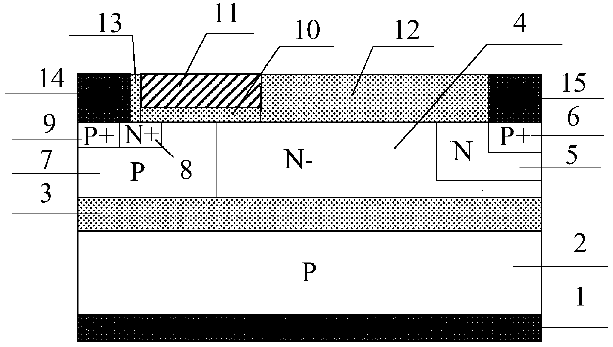
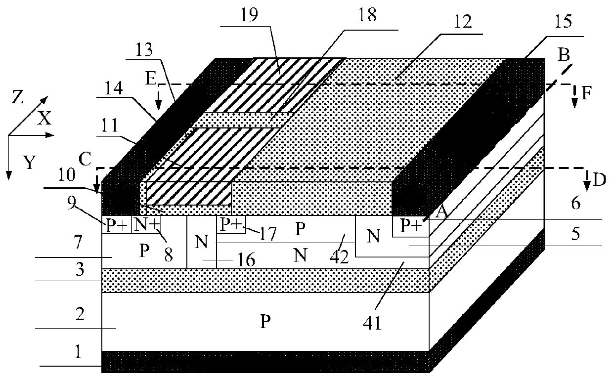
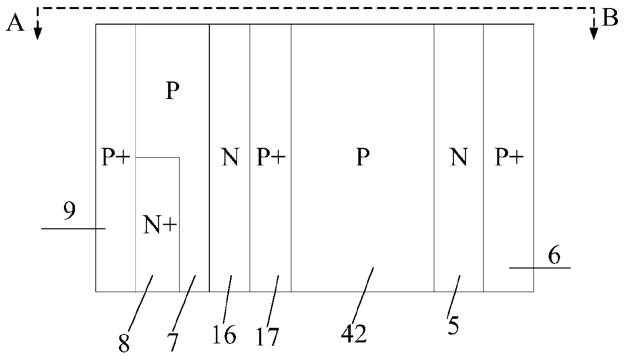
[0046] A lateral IGBT device embodiment, such as figure 2 As shown (the cross-sectional views along AB line, CD line and EF line are respectively shown in image 3 , Figure 4 and Figure 5 shown), comprising: a P-type semiconductor substrate 2, a substrate electrode 1 positioned on the lower surface of the P-type semiconductor substrate 2, and a buried oxide layer 3 positioned on the upper surface of the P-type semiconductor substrate 2, characterized in that the buried oxide layer A P-type base region 7, an N-type charge storage layer 16, and a superjunction N column 41 are arranged side by side on the upper surface. The width is 30-50 μm, the super junction N column 41 penetrates along the Z direction, and the doping concentration of the super junction N column 41 is 10 15 ~10 17 cm -3 ; In the P-type base region 7, there are N+ emitter regions 8 and P+ emitter regions 9 arranged side by side and mutually independent, and the junction depth between P+ emitter 9 and N+...
Embodiment 2
[0048] A lateral IGBT device embodiment, such as Figure 6 (Its cross-sectional views along AB line, CD line and EF line are as follows Figure 7 , Figure 8 and Figure 9 shown), comprising: a P-type semiconductor substrate 2, a substrate electrode 1 positioned on the lower surface of the P-type semiconductor substrate 2, and a buried oxide layer 3 positioned on the upper surface of the P-type semiconductor substrate 2, characterized in that the buried oxide layer A P-type base region 7, an N-type charge storage layer 16, and a superjunction N column 41 are arranged side by side on the upper surface. The width is 30-50 μm, the super junction N column 41 penetrates along the Z direction, and the doping concentration of the super junction N column 41 is 10 15 ~10 17 cm -3 ; In the P-type base region 7, there are arranged side by side and mutually independent N+ emitter regions 8 and P+ emitter regions 9. The region 9 runs through along the Z direction; inside the super ju...
Embodiment 3
[0050] A lateral IGBT device embodiment, such as Figure 10 (Its cross-sectional views along AB line, CD line and EF line are as follows Figure 11, Figure 12 and Figure 13 shown), on the basis of Embodiment 1, the separation gate electrode 19 is directly connected to the emitter metal 14 and the separation gate electrode 19 is surrounded by an L shape by adjusting the opening of the mask plate and steps such as photolithography, etching, and polycrystalline filling Gate electrode 11.
[0051] The direct equal potential between the separated gate electrode and the emitter metal makes the device not need additional metal wiring on the separated gate electrode, and the separated gate electrode of this shape can further reduce the gate capacitance, especially the Miller capacitance, and improve the performance of the device. switching speed, and can further shield the influence of the N-type charge storage layer on the breakdown voltage of the device.
PUM
| Property | Measurement | Unit |
|---|---|---|
| Width | aaaaa | aaaaa |
| Doping concentration | aaaaa | aaaaa |
| Doping concentration | aaaaa | aaaaa |
Abstract
Description
Claims
Application Information