
Method for preparing two-dimensional ultrathin silicon wafer loaded silver nanoparticles

A silver nanoparticle, ultra-thin technology, applied in the field of material chemistry, can solve the problems of application performance impact, complicated synthesis method steps, etc., and achieve the effect of simple steps

Inactive Publication Date: 2019-11-22
YANCHENG INST OF TECH
View PDF7 Cites 5 Cited by
  • Summary
  • Abstract
  • Description
  • Claims
  • Application Information

AI Technical Summary

Problems solved by technology

The main disadvantages of the above two methods are: (1) the silicon wafers used are all commercial single crystal silicon wafers, and the thickness is not at the nanometer level, which has a significant impact on the specific application performance; (2) the synthesis method used cumbersome steps

Method used


Image

  • Method for preparing two-dimensional ultrathin silicon wafer loaded silver nanoparticles
  • Method for preparing two-dimensional ultrathin silicon wafer loaded silver nanoparticles

Examples


Embodiment 1

[0028] A method for preparing two-dimensional ultrathin silicon wafers loaded with silver nanoparticles, comprising the following steps:

[0029] (1) Put 3g of calcium silicide in 300mL concentrated hydrochloric acid, react at -30°C for 5 days, filter, wash, and vacuum dry to obtain Si 6 h 6 Nanosheets.

[0030] (2) Dissolve silver nitrate in 10 mL of ethylenediamine to prepare a 0.1M silver nitrate solution in ethylenediamine.

[0031] (3) Add 0.1g Si 6 h 6 The nanosheets were ultrasonically dispersed in 10 mL of acetonitrile, 2 mL of silver nitrate ethylenediamine solution was added, reacted at 60 °C for 24 h at normal pressure, filtered and washed to obtain a composite material with silver nanoparticles loaded on the surface of two-dimensional ultra-thin silicon wafers.

Embodiment 2

[0033] A method for preparing two-dimensional ultrathin silicon wafers loaded with silver nanoparticles, comprising the following steps:

[0034] (1) Put 3g of calcium silicide in 300mL concentrated hydrochloric acid, react at -30°C for 5 days, filter, wash, and vacuum dry to obtain Si 6 h 6 Nanosheets.

[0035] (2) Dissolve silver nitrate in 10 mL of p-phenylenediamine to prepare a silver nitrate p-phenylenediamine solution with a concentration of 0.1M.

[0036] (3) Add 0.1g Si 6 h 6 Ultrasonically disperse the nanosheets in 10mL tetrahydrofuran, add 2mL silver nitrate p-phenylenediamine solution, react at room temperature to 60°C under normal pressure for 1-24h, filter and wash to obtain two-dimensional ultra-thin silicon wafers loaded with silver nanoparticles Granular composites.

Embodiment 3

[0038] A method for preparing two-dimensional ultrathin silicon wafers loaded with silver nanoparticles, comprising the following steps:

[0039] (1) Put 3g of calcium silicide in 300mL concentrated hydrochloric acid, react at -30°C for 5 days, filter, wash, and vacuum dry to obtain Si 6 h 6 Nanosheets.

[0040] (2) Dissolve silver nitrate in 10 mL of tri-n-propylamine to prepare a solution of silver nitrate in tri-n-propylamine with a concentration of 0.1M.

[0041] (3) Add 0.1~1g Si 6 h 6 Ultrasonically disperse nanosheets in 10mL tetrahydrofuran, add 1-10mL silver nitrate tri-n-propylamine solution, react at room temperature to 60°C under normal pressure for 1-24h, filter and wash to obtain two-dimensional ultra-thin silicon wafer surface loaded with silver Composite materials of nanoparticles.


PUM


Abstract

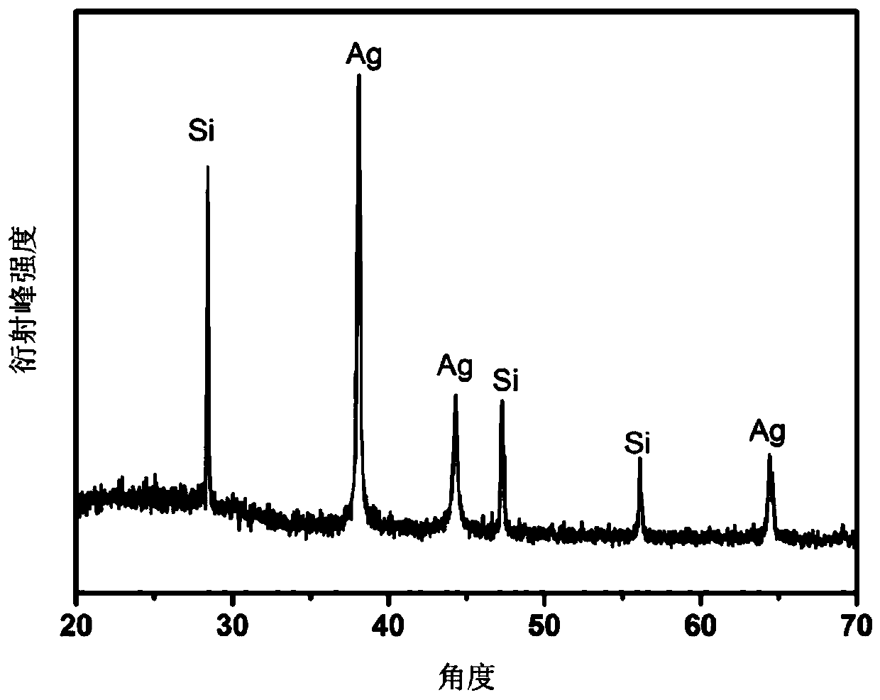
The invention discloses a method for preparing two-dimensional ultrathin silicon wafer loaded silver nanoparticles. The method includes the following steps that firstly, calcium silicide is put into concentrated hydrochloric acid to be reacted, filtered and washed, vacuum drying is conducted, and a Si6H6 nano sheet is obtained; secondly, silver nitrate is dissolved into amine which can form a complexing effect with Ag+, and a silver nitrate amine solution is prepared; and thirdly, the Si6H6 nano sheet is ultrasonically dispersed in an organic solvent and is added to the silver nitrate amine solution, reacting, filtering and washing are conducted, and a two-dimensional ultrathin silicon wafer loaded silver nanoparticle composite material is obtained. By means of the method, the concentratedhydrochloric acid and the layered compound calcium silicide are reacted to generate the Si6H6 nano sheet, then the Si6H6 nano sheet is added to a silver nitrate and amine complex compound, and the two-dimensional ultrathin silicon wafer loaded silver nanoparticle composite material is obtained through a one-step reaction. The steps are simple, operation is easy, and the obtained composite material has potential application in the field of high-magnification lithium ion batteries.

Description

technical field [0001] The invention belongs to the field of material chemistry, and in particular relates to a method for preparing two-dimensional ultrathin silicon chips loaded with silver nanoparticles. Background technique [0002] Since the discovery of graphene materials in 2004, two-dimensional flake nanomaterials have received extensive attention and research due to their potential excellent physical and chemical properties. Silicon and carbon share the same main group, and silicon has been widely used in the fields of microelectronics and solar cells. Therefore, two-dimensional ultra-thin nano-silicon materials have received more and more attention. However, since silicon is a semiconductor material, its inherently poor conductivity hinders its application in photoelectrocatalysis, high-rate lithium-ion batteries and other fields. How to improve the conductivity and photoelectrochemical activity of two-dimensional silicon nanomaterials is still a thorny issue. As...

Claims


Application Information

Patent Timeline
IPC IPC(8): B22F9/24B22F1/00C01B33/027H01M4/36H01M4/38H01M10/0525
CPCB22F9/24C01B33/027H01M4/362H01M4/38H01M4/386H01M10/0525H01M2004/027B22F1/054Y02E60/10
Inventor 孙林谢杰黄松超刘涛吴俊姜瑞雨吴兵
Owner YANCHENG INST OF TECH
Learn More