IGBT with self-biased separation gate structure

A separate gate and self-bias technology, which is applied in the direction of electrical components, circuits, semiconductor devices, etc., can solve the problem of slow switching speed of devices, achieve the effects of reducing switching loss, increasing switching speed, and reducing gate capacitance

Active Publication Date: 2019-11-22
UNIV OF ELECTRONICS SCI & TECH OF CHINA
View PDF11 Cites 10 Cited by
  • Summary
  • Abstract
  • Description
  • Claims
  • Application Information

AI Technical Summary

Problems solved by technology

However, the increase of the trench gate depth will increase the gate capacitance of the...

Method used


Image

  • IGBT with self-biased separation gate structure
  • IGBT with self-biased separation gate structure
  • IGBT with self-biased separation gate structure

Examples


Embodiment 1

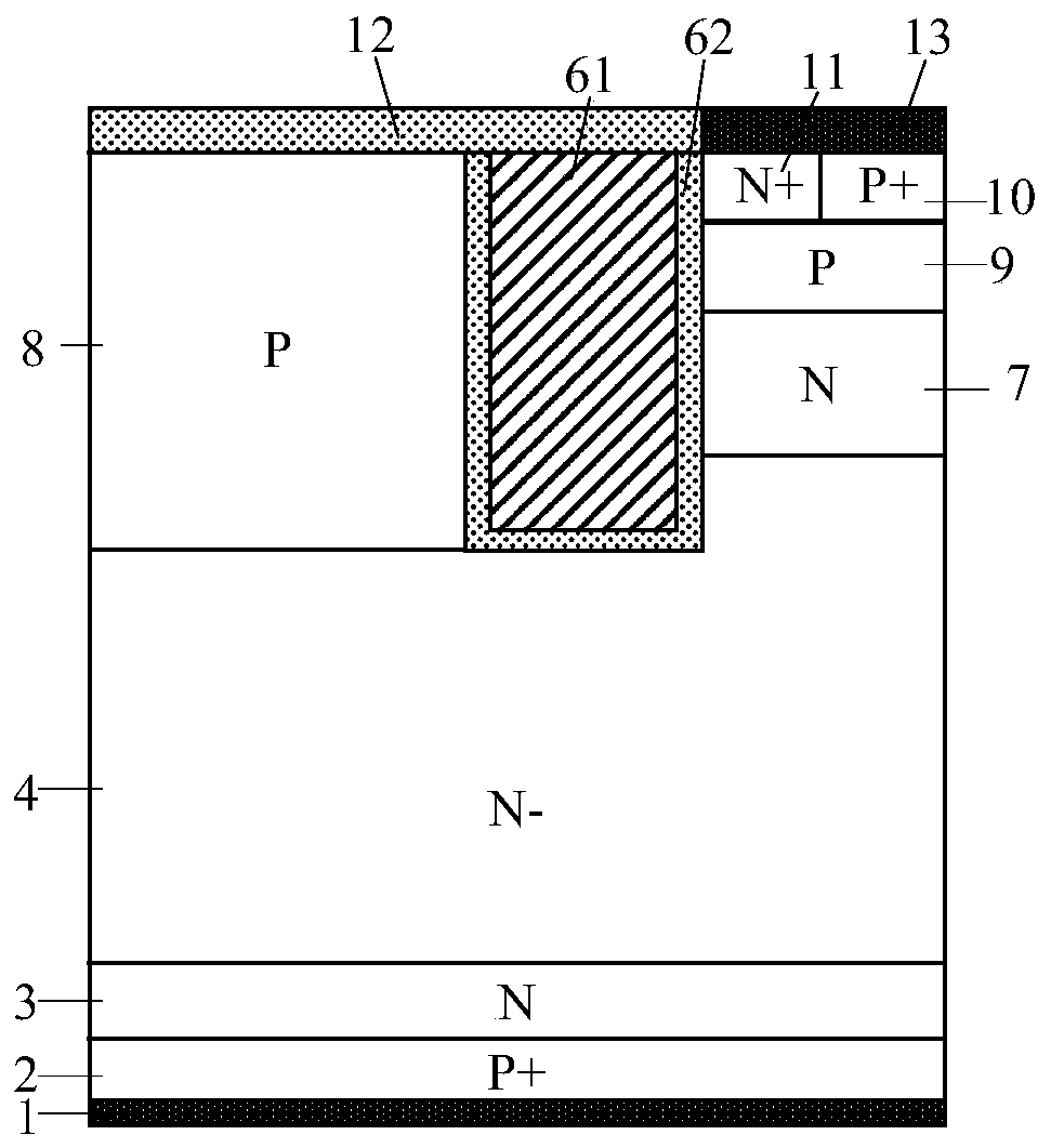
[0024] An IGBT with a self-biased split gate structure, its half-cell structure is as follows figure 2 As shown, it includes collector metal 1; N-type field stop layer 2 located on the upper surface of collector metal 1; N-drift region 4 located above N-type field stop layer 3; The P-type floating region 8; the metal 142 located on the upper surface of the P-type floating region 8; the N-type charge storage layer 7 located on the other side above the N-drift region, and the doping concentration of the N-type charge storage layer is greater than or Equal to the doping concentration of the N-drift region 4; the P-type base region 9 located on the upper surface of the N-type charge storage layer; the N+ emitter region 11 and the P+ emitter region 10 located side by side on the upper surface of the P-type base region 9 and independent of each other; The emitter metal 13 on the upper surface of the N+ emitter region 11 and the P+ emitter region 10; the trench structure on one side...

Embodiment 2

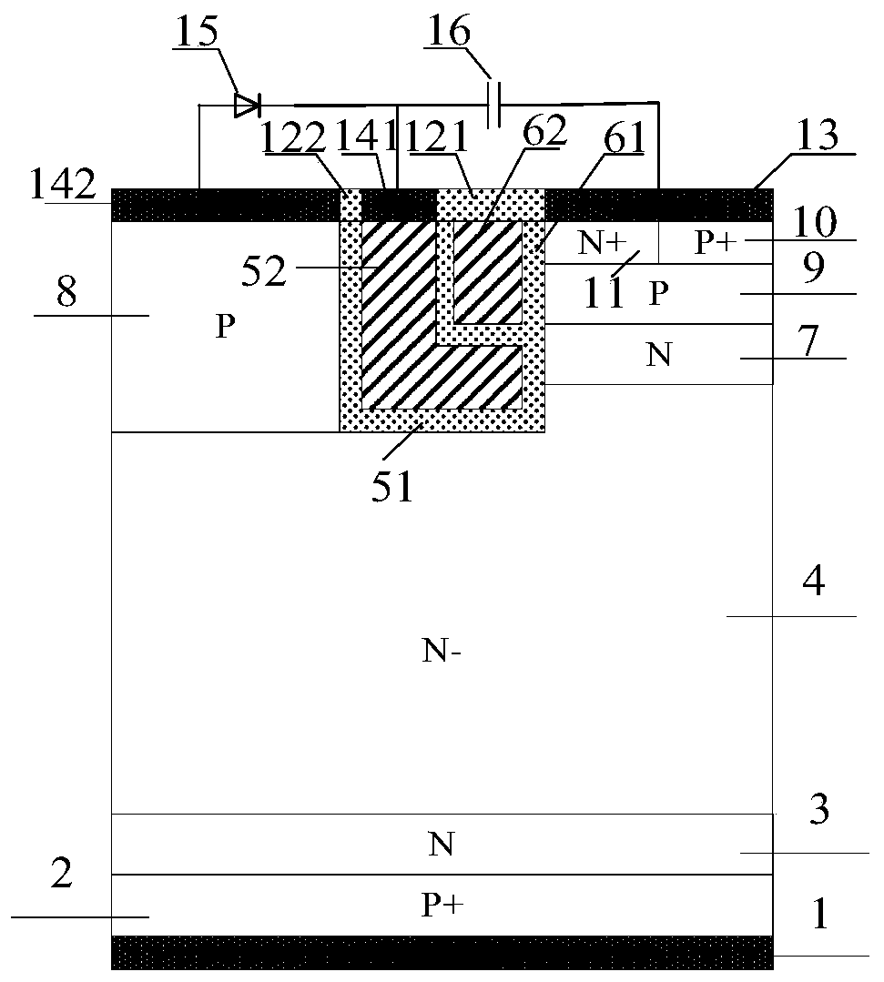
[0026] An IGBT with a self-biased split gate structure, its half-cell structure is as follows figure 2As shown, it includes collector metal 1; N-type field stop layer 2 located on the upper surface of collector metal 1; N-drift region 4 located above N-type field stop layer 3; The P-type floating region 8; the metal 142 located on the upper surface of the P-type floating region 8; the N-type charge storage layer 7 located on the other side above the N-drift region; the P-type base region located on the upper surface of the N-type charge storage layer 9; N+ emitter regions 11 and P+ emitter regions 10 placed side by side on the upper surface of the P-type base region 9 and independent of each other; emitter metal 13 located on the upper surfaces of the N+ emitter region 11 and P+ emitter region 10; located in the P-type floating region The trench structure on one side includes a separation gate dielectric layer 51, a separation gate electrode 52, the depth of the separation ga...

Embodiment 3

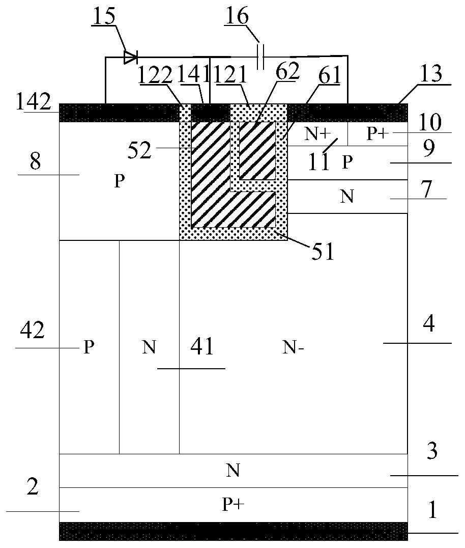
[0028] An IGBT with a self-biased split-gate structure with a half-cell structure such as Figure 4 As shown, on the basis of Embodiment 1, the diode 15 is integrated on the surface of the IGBT, and the P+ region 151 and the N+ region 152 that are placed side by side on the upper surface of the medium 122 and are independent from each other, and the metal 142 connected to the P+ region 151, and the N+ region 152 Connected metal 142 forms a diode.

[0029] Integrating the diode 15 into the IGBT reduces the packaging area of ​​the chip and improves the integration of the chip.


PUM


Abstract

The invention belongs to the technical field of power semiconductor devices, and relates to a separation gate TIGBT with a self-biased PMOS and a manufacturing method thereof. According to the invention, a PMOS structure is introduced on the basis of a traditional TIGBT; the channel density is not reduced; saturation current during forward conduction of the device is effectively improved, the short-circuit safety working capability of the device is improved, and meanwhile, an extra current discharge path provided by the PMOS structure accelerates the hole extraction speed of the device in a blocking state, so that the switching speed of the device is increased, and the switching loss of the device is reduced. Meanwhile, for the TIGBT with an N-type charge storage layer, a P-type buried layer can shield the influence of the N-type charge storage layer on the breakdown characteristic of the device; therefore, the doping concentration of the N-type charge storage layer can be improved tofurther improve the carrier distribution during forward conduction of the device, the conductivity modulation capability of a drift region is improved, and the compromise relationship between the forward conduction voltage drop Vce (on) and the turn-off loss Eoff of the device is further improved.

Description

technical field [0001] The invention belongs to the technical field of power semiconductor devices, and relates to an IGBT with a self-biased separation gate structure. Background technique [0002] Insulated Gate Bipolar Transistor (IGBT) is one of the fastest growing electronic power devices today. Compared with traditional transistors and MOSFETs, it has the advantages of both transistors and MOSFETs. It not only has the advantages of high input impedance, low control power, simple driving circuit, fast switching speed, and low switching loss of MOSFET; it also has the advantages of bipolar Power transistors have the advantages of high current density, low saturation voltage drop, high current handling capability, and good stability, so they are widely used in high-voltage, high-current and other fields. [0003] Since the IGBT came out in the early 1980s, after more than 30 years of development, the manufacturing level of the structure of the IGBT device has been contin...

Claims


Application Information

Patent Timeline
IPC IPC(8): H01L29/739H01L21/331H01L29/06
CPCH01L29/0615H01L29/66325H01L29/7393
Inventor 张金平王康赵阳刘竞秀李泽宏张波
Owner UNIV OF ELECTRONICS SCI & TECH OF CHINA
Why Eureka
Try Eureka