Packaging structure forming method

A technology of packaging structure and contact structure, which is applied in the manufacturing of electrical components, electric solid-state devices, semiconductor/solid-state devices, etc., can solve the problem that the electromagnetic shielding effect needs to be improved, and achieve the effect of improving efficiency

Active Publication Date: 2019-11-26
NANTONG TONGFU MICROELECTRONICS CO LTD
View PDF5 Cites 1 Cited by
  • Summary
  • Abstract
  • Description
  • Claims
  • Application Information

AI Technical Summary

Problems solved by technology

[0004] An existing electromagnetic shielding solution is mainly to set a magnetic field shielding layer on the semiconductor packaging structure to shield the electromagnetic interference between chips, but the effect of the existing electromagnetic shielding still needs to be improved

Method used


Image

  • Packaging structure forming method
  • Packaging structure forming method
  • Packaging structure forming method

Examples


Embodiment Construction

[0039] As mentioned in the background, the effect of existing electromagnetic shielding still needs to be improved.

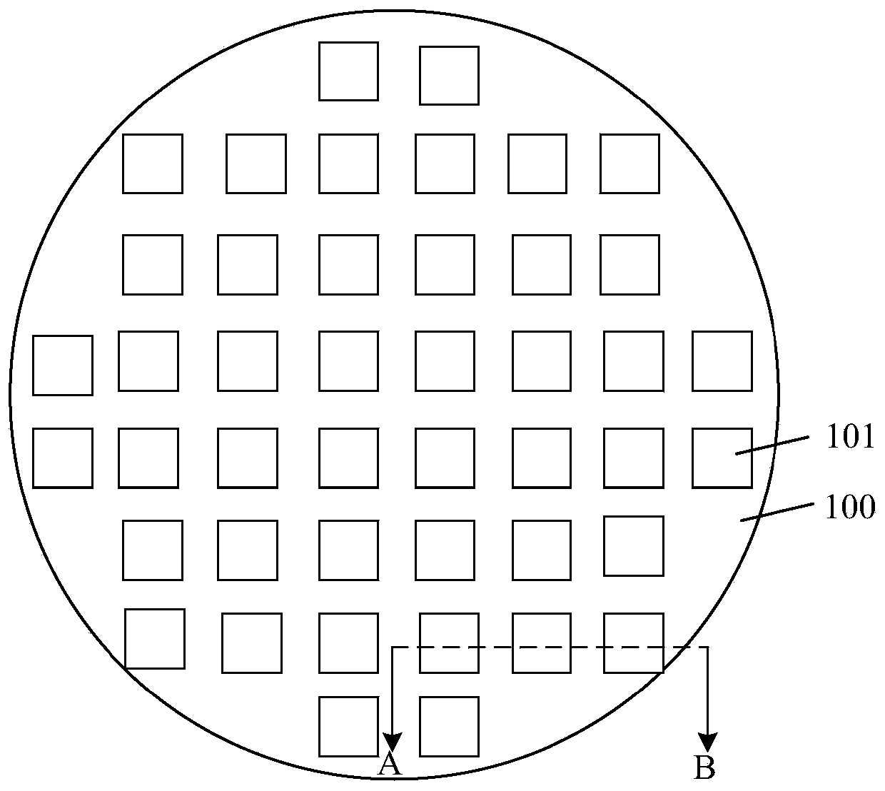
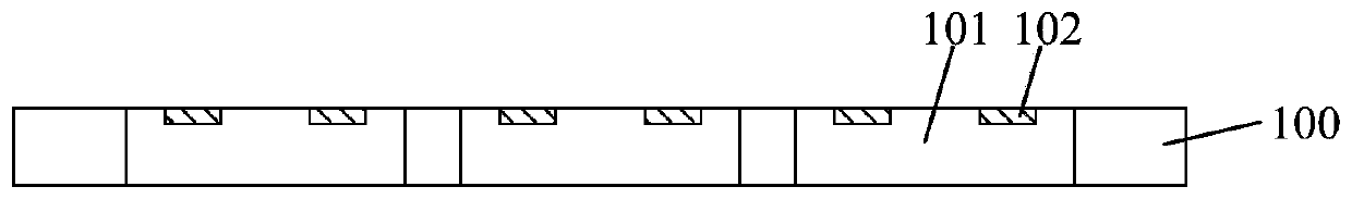
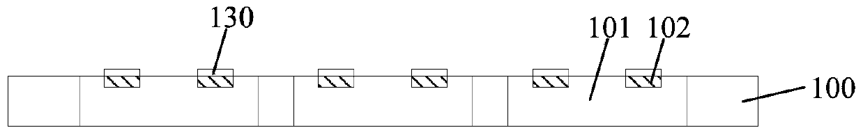
[0040] The study found that the existing magnetic field shielding layer is generally formed by sputtering process. Since the thickness of the semiconductor package structure is generally thick, and the semiconductor package structure is generally rectangular, the semiconductor package structure has multiple corners and the side wall is relatively steep. When the magnetic field shielding layer covering the semiconductor package structure is formed by sputtering, the thickness of the formed magnetic field shielding layer is likely to be uneven, and the edge of the semiconductor package structure may not be covered, thus making it difficult to guarantee the shielding effect of the magnetic field shielding layer.

[0041] Therefore, the present invention provides a packaging structure and a forming method thereof. In the forming method, after the first plastic seali...


PUM


Abstract

The invention discloses a packaging structure forming method. The packaging structure forming method comprises the following steps: a first shielding layer covering semiconductor chips is formed afterfirst plastic package layers on the functional surfaces of a number of semiconductor chips are adhered to a carrier board, and the surface of the first shielding layer is ellipsoid-shaped; a second shielding layer is formed on the first shielding layer; a second plastic package layer is formed on the second shielding layer and the carrier board among the semiconductor chips; the carrier board ispeeled, and a pre-packaging panel is formed; and an external contact structure connected with a metal bump is formed on the back of the pre-packaging panel. Through the formed first shielding layer with an ellipsoidal surface, not only the first shielding layer itself can evenly and completely cover the non-functional surfaces and the side wall surfaces of the semiconductor chips, but also the second shielding layer cannot have the problems of uneven thickness and poor edge coverage when the second shielding layer is formed; therefore, the overall shielding layer formed by both the first shielding layer and the formed second shielding layer is complete, and the shielding effect is improved.

Description

technical field [0001] The invention relates to the field of semiconductor manufacturing, in particular to a method for forming a packaging structure with electromagnetic shielding. Background technique [0002] The rapid development of a new generation of electronic products has promoted the development of integrated circuit packaging in the direction of high density, high frequency, miniaturization, and high integration, and high-frequency chips often generate strong electromagnetic waves, which cause undesirable effects on the inside and outside of the package and the chip. In addition, the density of electronic components is getting higher and higher, and the distance of transmission lines is getting closer and closer, which makes the problem of electromagnetic interference from inside and outside the integrated circuit package more and more serious, and at the same time will reduce the quality and life of integrated circuits. [0003] In electronic equipment and electro...

Claims


Application Information

Patent Timeline
Patent Type & Authority Applications(China)
IPC IPC(8): H01L21/56H01L21/60H01L23/552H01L23/31
CPCH01L21/561H01L21/568H01L23/3107H01L23/552H01L24/02H01L24/03H01L24/11H01L24/97H01L2224/0231H01L2224/02379H01L2224/0401H01L2224/18
Inventor 陶玉娟
Owner NANTONG TONGFU MICROELECTRONICS CO LTD
Why Eureka
Try Eureka