Integrated power semiconductor device and manufacturing method thereof

A semiconductor and success rate technology, applied in the field of integrated power semiconductor devices and their manufacturing, which can solve the problems of excessive chip leakage current and low manufacturing cost.

Active Publication Date: 2019-12-10
UNIV OF ELECTRONIC SCI & TECH OF CHINA
View PDF6 Cites 5 Cited by
  • Summary
  • Abstract
  • Description
  • Claims
  • Application Information

AI Technical Summary

Problems solved by technology

Based on the principle of RESURF withstand voltage, we have invented the BCD semiconductor device and its manufacturing technology (patent number: ZL200810148118.3), realizing the monolithic integration of nLIGBT, nLDMOS, low-voltage NMOS, low-voltage PMOS and low-voltage NPN on a single

Method used


Image

  • Integrated power semiconductor device and manufacturing method thereof
  • Integrated power semiconductor device and manufacturing method thereof
  • Integrated power semiconductor device and manufacturing method thereof

Examples


Embodiment 1

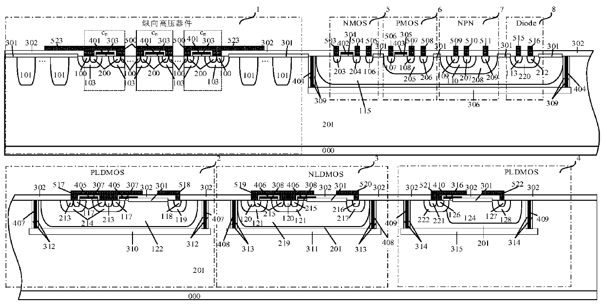
[0122] Such as figure 1 As shown, an integratable power semiconductor device includes a vertical high-voltage device 1, a first high-voltage pLDMOS device 2, a high-voltage nLDMOS device 3, a second high-voltage pLDMOS device 4, a low-voltage NMOS device 5, and a low-voltage PMOS device integrated on the same chip. 6. Low-voltage NPN device 7 and low-voltage Diode device 8, the first high-voltage pLDMOS device 2, high-voltage nLDMOS device 3, second high-voltage pLDMOS device 4, low-voltage NMOS device 5, low-voltage PMOS device 6, low-voltage NPN device 7 and low-voltage Diode Dielectric isolation is used between the devices 8 to realize complete isolation of high-voltage devices and low-voltage devices. The first high-voltage pLDMOS device 2 and the high-voltage nLDMOS device 3 adopt a multi-channel design, and the second high-voltage pLDMOS device 4 adopts a single-channel design;

[0123] The vertical high voltage device 1 includes a substrate 000, a second conductivity ty...

Embodiment 2

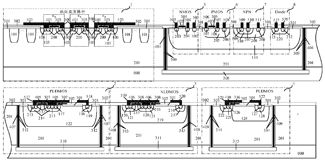
[0135] Such as figure 2 As shown, the difference between this embodiment and Embodiment 1 is that the first oxygen injection layer 306 , the second oxygen injection layer 310 , the third oxygen injection layer 311 and the fourth oxygen injection layer 315 are located inside the substrate 000 .

[0136] Such as Figure 17 As shown, the manufacturing method of the integrated power semiconductor device of this embodiment includes the following steps:

[0137] The first step is to use substrate 000;

[0138] In the second step, a certain amount of oxygen ions is implanted into the substrate 000 by photolithography and ion implantation;

[0139] The third step is annealing to form the first oxygen injection layer 306, the second oxygen injection layer 310, and the third oxygen injection layer 311;

[0140] The fourth step is to epitaxially form the epitaxial layer 201 of the second conductivity type;

[0141] The fifth step is to form a dielectric groove by using a deep groove...

Embodiment 3

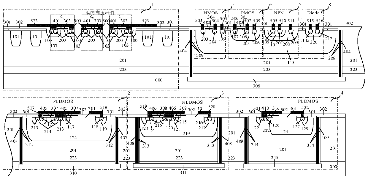
[0149] Such as image 3 As shown, the difference between this embodiment and Embodiment 2 is that: in the vertical high voltage device 1 , a field resistance layer 223 of the second conductivity type is inserted between the substrate 000 and the epitaxial layer 201 of the second conductivity type.


PUM


Abstract

The invention provides an integrated power semiconductor device and a manufacturing method thereof. The semiconductor device comprises a longitudinal high-voltage device, a first high-voltage pLDMOS device, a high-voltage nLDMOS device, a second high-voltage pLDMOS device, a low-voltage NMOS device, a low-voltage PMOS device, a low-voltage NPN device and a low-voltage Diode device which are integrated on the same chip. The first high-voltage pLDMOS device, the high-voltage nLDMOS device, the second high-voltage pLDMOS device, the low-voltage NMOS device, the low-voltage PMOS device, the low-voltage NPN device and the low-voltage Diode device are all isolated through media. The first high-voltage pLDMOS device and the high-voltage nLDMOS device adopt a multi-channel design, and the second high-voltage pLDMOS device adopts a single-channel design. The invention provides a partial oxygen burying integration technology, an oxygen burying layer is formed by adopting ion implantation and other modes, the technology can integrate a transverse high-voltage device, the longitudinal high-voltage device and a low-voltage device, and problems of current leakage and crosstalk are avoided. Compared with the transverse high-voltage device, by using the semiconductor device of the invention, an on-resistance is low and an occupied chip area is small.

Description

technical field [0001] The invention belongs to the technical field of semiconductor power devices, and relates to an integrated power semiconductor device and a manufacturing method thereof. Background technique [0002] High-voltage power integrated circuits often use the high analog precision of Bipolar transistors, the high integration of CMOS, and the high power or voltage characteristics of DMOS (Double-diffused MOSFET) to integrate Bipolar analog circuits, CMOS logic circuits, CMOS analog circuits and DMOS high-voltage power devices. Monolithically integrated together (referred to as BCD process). BCD process integration technology is a commonly used monolithic integration technology, which can greatly reduce system power loss, improve system performance, save circuit packaging costs and have better reliability. [0003] Lateral high-voltage devices are widely used in high-voltage power integrated circuits because the drain, gate, and source are all on the chip surfa...

Claims


Application Information

Patent Timeline
IPC IPC(8): H01L27/12H01L21/84
CPCH01L27/1207H01L21/84H01L21/76267H01L29/78H01L29/7802H01L29/7824H01L29/42368H01L29/7831H01L29/0878H01L29/402H01L29/7811H01L29/0619H01L29/0634H01L29/66681H01L29/66712H01L27/0635H01L27/0922H01L21/823878H01L21/823885H01L29/407H01L29/7395H01L29/735H01L29/66333H01L21/76283H01L21/76224H01L21/823807H01L21/823814H01L21/823828H01L21/823857H01L21/823871H01L21/823892H01L29/7396H01L29/7803H01L29/7817H01L29/7832
Inventor 乔明何林蓉李怡赖春兰张波
Owner UNIV OF ELECTRONIC SCI & TECH OF CHINA
Why Eureka
Try Eureka