
Etching method of opening with high depth-to-width ratio and semiconductor device

A high aspect ratio, semiconductor technology, used in semiconductor devices, semiconductor/solid-state device manufacturing, electrical solid-state devices, etc., can solve the problems of stripes on the sidewalls of openings, unsatisfactory opening contours, and decreased etching ability, and achieve etching Ability to improve, reduce temperature, and evenly distribute the effects

Active Publication Date: 2019-12-13
YANGTZE MEMORY TECH CO LTD
View PDF5 Cites 2 Cited by
  • Summary
  • Abstract
  • Description
  • Claims
  • Application Information

AI Technical Summary

Problems solved by technology

[0004] In the current etching of high-aspect-ratio openings, the opening profile is not ideal, for example, there are problems such as opening bowing and opening sidewall striation.
In addition, when the aspect ratio of the opening is further increased, the etching ability will decrease, and the predetermined depth cannot be reached.

Method used


Image

  • Etching method of opening with high depth-to-width ratio and semiconductor device
  • Etching method of opening with high depth-to-width ratio and semiconductor device
  • Etching method of opening with high depth-to-width ratio and semiconductor device

Examples


Embodiment Construction

[0037] In order to make the above objects, features and advantages of the present invention more clearly understood, the specific embodiments of the present invention will be described in detail below with reference to the accompanying drawings.

[0038] Numerous specific details are set forth in the following description to facilitate a full understanding of the present invention, but the present invention may also be implemented in other ways than those described herein, and thus the present invention is not limited by the specific embodiments disclosed below.

[0039] As shown in this application and in the claims, unless the context clearly dictates otherwise, the words "a", "an", "an" and / or "the" are not intended to be specific in the singular and may include the plural. Generally speaking, the terms "comprising" and "comprising" only imply that the clearly identified steps and elements are included, and these steps and elements do not constitute an exclusive list, and th...


PUM

PropertyMeasurementUnit
Thicknessaaaaaaaaaa

Abstract

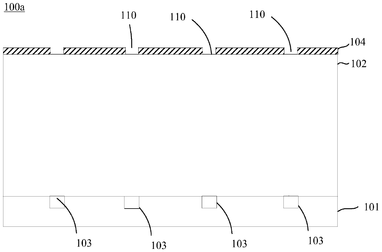
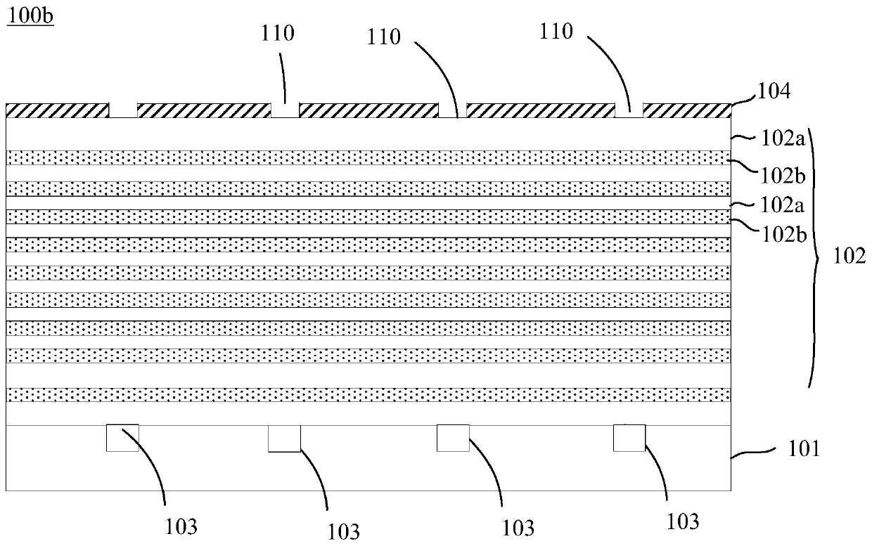
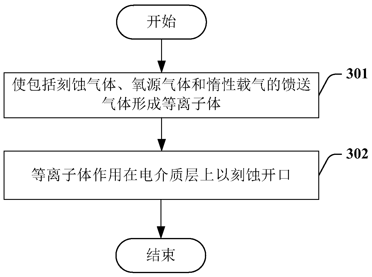
The invention relates to an etching method of an opening with a high depth-to-width ratio and a semiconductor device. The etching method of an opening with a high depth-to-width ratio comprises the step of dry-etching a dielectric layer by using a feed gas including an etching gas, an oxygen source gas and an inert carrier gas to form an opening, wherein the flow proportion of the inert carrier gas in the feed gas is 4-21%.

Description

technical field [0001] The present invention mainly relates to a semiconductor manufacturing method, in particular to an etching method of a high aspect ratio opening and a semiconductor device. Background technique [0002] Opening etching is a key technology of VLSI. As CMOS devices enter the post-32nm process era, high aspect ratio opening etching and its filling have a considerable impact on the yield of the device. For advanced memories, aspect ratios have reached over 40:1, which makes the challenge even greater. [0003] In semiconductor devices such as NAND memory, DRAM memory or CMOS devices, the medium through which the openings are etched is usually silicon dioxide (SiO 2 ), silicon nitride (SixNy, such as Si 3 N 4 ), silicon oxynitride (SiOxNy) and other insulating layers. The openings may be holes or trenches. For holes, the dimensions in the two horizontal directions are similar or in the same order of magnitude. For a trench, the dimension in one horizon...

Claims


Application Information

Patent Timeline
IPC IPC(8): H01L21/311H01L21/768H01L27/092
CPCH01L21/31116H01L21/76802H01L27/092H01L2221/101
Inventor 王猛黄海辉左明光曾最新朱宏斌霍宗亮程卫华
Owner YANGTZE MEMORY TECH CO LTD
Learn More