

GaN-based fin field effect transistor device and manufacturing method thereof
A fin-type field effect and manufacturing method technology, applied in the field of electronics, can solve the problems of small space for performance improvement and insufficient linearity, and achieve the effects of improving linearity, reducing electric field intensity, and uniform electric field distribution
- Summary
- Abstract
- Description
- Claims
- Application Information
AI Technical Summary
Problems solved by technology
Method used
Image

Examples
Embodiment Construction
[0044] In order to make the above objects, features and advantages of the present invention more comprehensible, specific implementations of the present invention will be described in detail below in conjunction with the accompanying drawings.
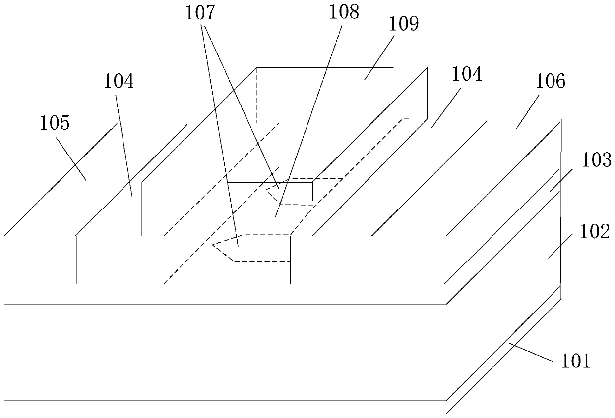
[0045] The present invention firstly provides a GaN-based fin field effect transistor device, the structure of which is as follows figure 1 As shown, it includes a substrate 101, a buffer layer 102, a barrier layer 103, and a passivation layer 104 arranged in sequence, wherein:
[0046] The barrier layer 103 is provided with a source 105 at one end and a drain 106 at the other end;
[0047] The passivation layer 104 is disposed on the barrier layer 103 between the source 105 and the drain 106; an opening is disposed in the middle of the passivation layer 104;
[0048] A plurality of grooves 107 are arranged in the region of the barrier layer 103 corresponding to the opening; fins 108 are arranged between adjacent grooves 107;
[0049...
PUM
 Abstract
Description
Claims
Application Information