
An apparatus using multiple beams of charged particles

A technology of charged particle beams and equipment, applied in the direction of circuits, discharge tubes, electrical components, etc., can solve problems such as pattern defects, connection failures or separation failures

Active Publication Date: 2019-12-13
ASML NETHERLANDS BV
View PDF12 Cites 0 Cited by
  • Summary
  • Abstract
  • Description
  • Claims
  • Application Information

AI Technical Summary

Problems solved by technology

Inspection may also reveal patterning defects (e.g., failed attachment or detachment) and uninvited particles

Method used


Image

  • An apparatus using multiple beams of charged particles
  • An apparatus using multiple beams of charged particles
  • An apparatus using multiple beams of charged particles

Examples


Embodiment Construction

[0056] Various techniques exist for inspecting samples (eg, substrates and patterned devices). One inspection technique is optical inspection, where a beam of light is directed to a substrate or patterning device, and a signal is recorded representing the interaction of the beam with the sample (eg, scattering, reflection, diffraction). Another inspection technique is charged particle beam inspection, in which a beam of charged particles (eg, electrons) is directed to a sample and signals representing interactions of the charged particles with the sample (eg, secondary and backscattered emissions) are recorded.

[0057] Charged particle beam inspection can have higher resolution than optical inspection because the charged particles used in the former have a shorter wavelength than the light used in the latter. Charged particle beam inspection is becoming more widely used as the dimensions of patterns on substrates and patterned devices become smaller as device fabrication proc...


PUM


Abstract

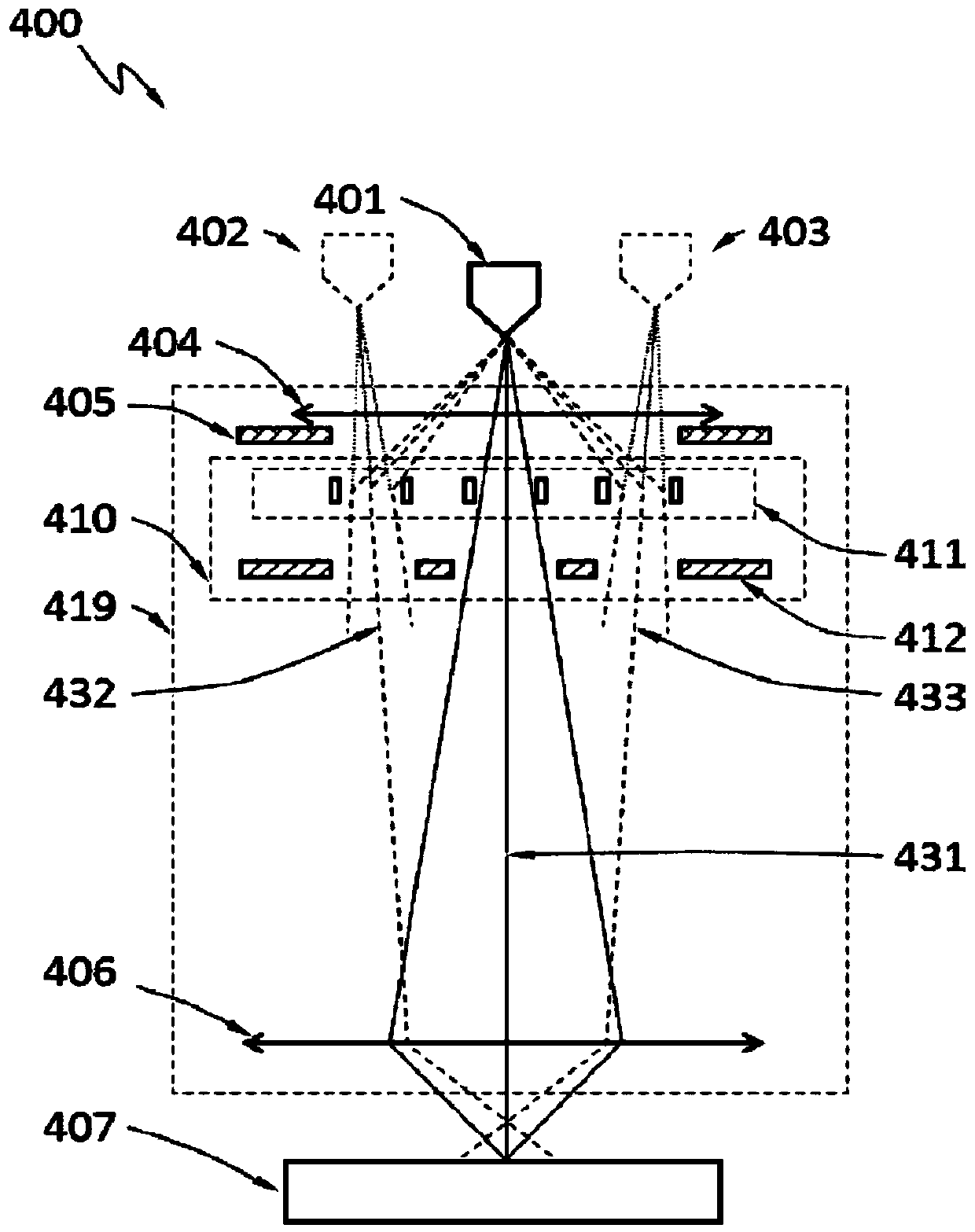
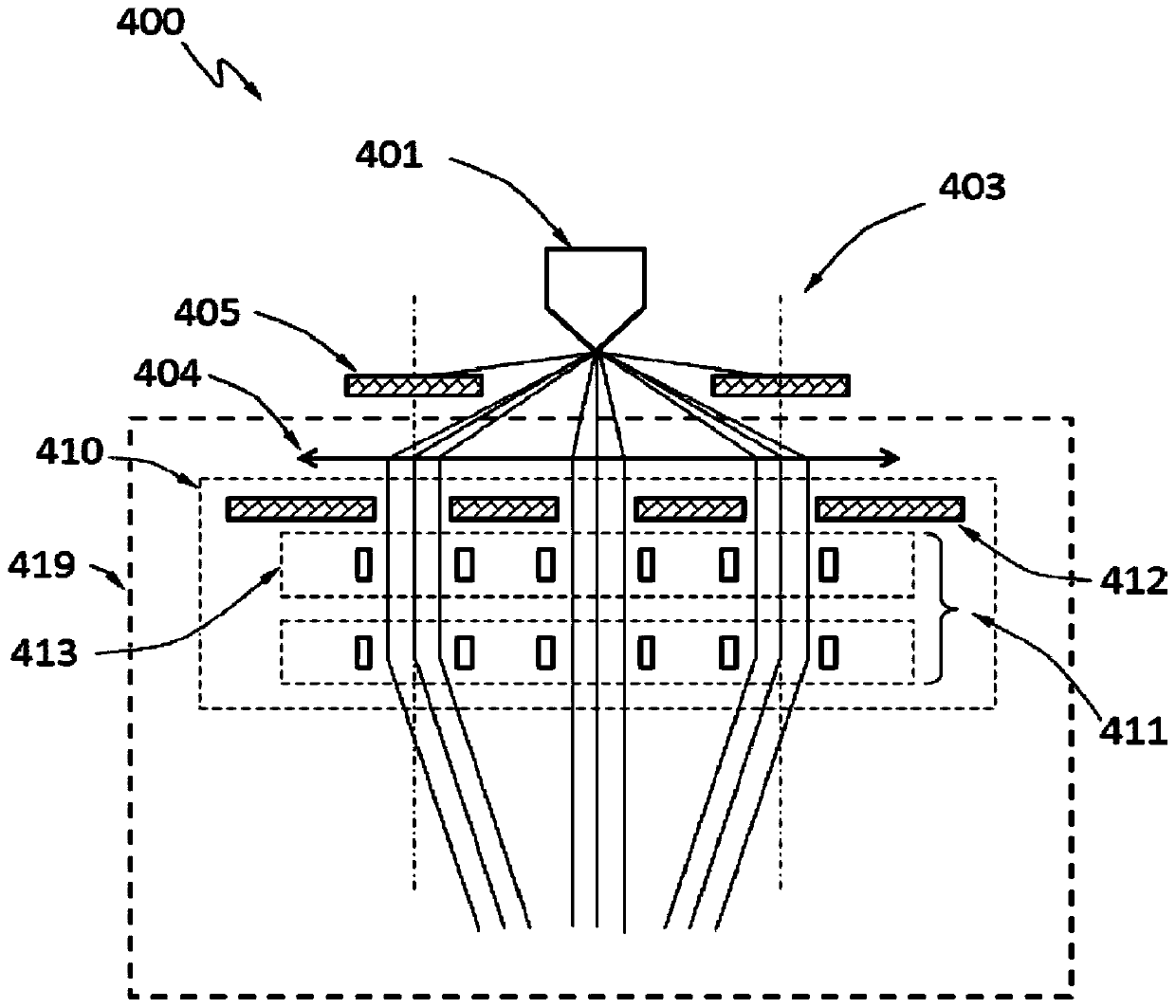
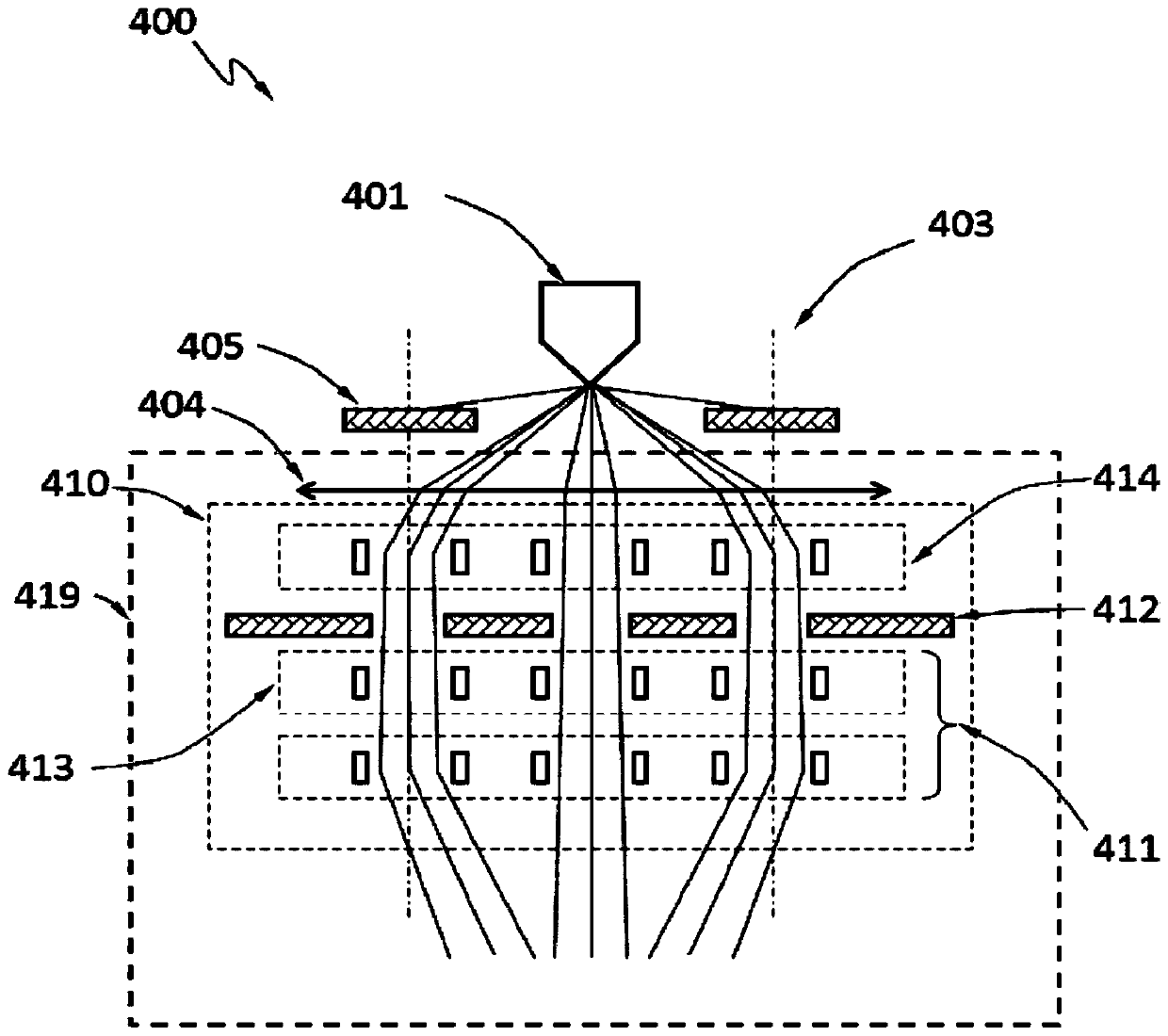
Disclosed herein is an apparatus comprising: a first electrically conductive layer; a second electrically conductive layer; a plurality of optics element s between the first electrically conductive layer and the second electrically conductive layer, wherein the plurality of optics elements are configured to influence a plurality of beams of charged particles; a third electrically conductive layerbetween the first electrically conductive layer and the second electrically conductive layer; and an electrically insulating layer physically connected to the optics elements, wherein the electricallyinsulating layer is configured to electrically insulate the optics elements from the first electrically conductive layer, and the second electrically conductive layer.

Description

[0001] Cross References to Related Applications [0002] This application claims priority to US Application 62 / 492,043, filed April 28, 2017, the entire contents of which are incorporated herein by reference. technical field [0003] The present disclosure relates to an apparatus for inspecting or observing samples, such as wafers and masks, used in device fabrication processes, such as the fabrication of integrated circuits (ICs). Background technique [0004] The device fabrication process may include applying a desired pattern to a substrate. A patterning device (alternatively referred to as a mask or reticle) can be used to generate the desired pattern. The pattern can be transferred onto a target portion (eg, a portion comprising one or several dies) on a substrate (eg, a silicon wafer). The transfer of the pattern is usually via imaging onto a layer of radiation sensitive material (resist) provided on the substrate. A single substrate may contain a network of adjac...

Claims


Application Information

Patent Timeline
IPC IPC(8): H01J37/317H01J37/147H01J37/12
CPCH01J37/12H01J37/1472H01J37/3177H01J2237/0213H01J2237/0262H01J2237/032H01J2237/038H01J2237/0435H01J2237/1205H01J37/1477H01J37/26
Inventor 胡学让任伟明刘学东陈仲玮
Owner ASML NETHERLANDS BV
Learn More