SMT surface mounting process

A patch and process technology, applied in the direction of epoxy resin glue, adhesive type, adhesive additives, etc., can solve the problems of slow curing speed, complex process, low product qualification rate, etc., to improve production efficiency, bonding The effect of high strength and fast packaging speed

Active Publication Date: 2019-12-20
东莞市合权电子有限公司
View PDF10 Cites 1 Cited by
  • Summary
  • Abstract
  • Description
  • Claims
  • Application Information

AI Technical Summary

Problems solved by technology

[0003] The SMT patching process in the prior art has defects such as complex process, low product qualification rate, low efficiency, low bonding strength of the patch adhesive, and slow curing speed.

Method used


Image

  • SMT surface mounting process
  • SMT surface mounting process
  • SMT surface mounting process

Examples


Embodiment 1

[0024] A kind of SMT patch technology, comprises the steps:

[0025] (1) Pretreatment: cleaning and drying the PCB board;

[0026] (2) Glue dispensing: use a glue dispenser to apply patch glue to the preset glue dispensing position on the PCB;

[0027] (3) SMT: use a SMT machine to mount the components on the PCB;

[0028] (4) Curing: Send the PCB board into the curing equipment and cure it at 130°C for 2 minutes;

[0029] (5) Reflow soldering: send the PCB board into the reflow soldering furnace for reflow soldering;

[0030] (6) Inspection: check the yield rate of the finished product.

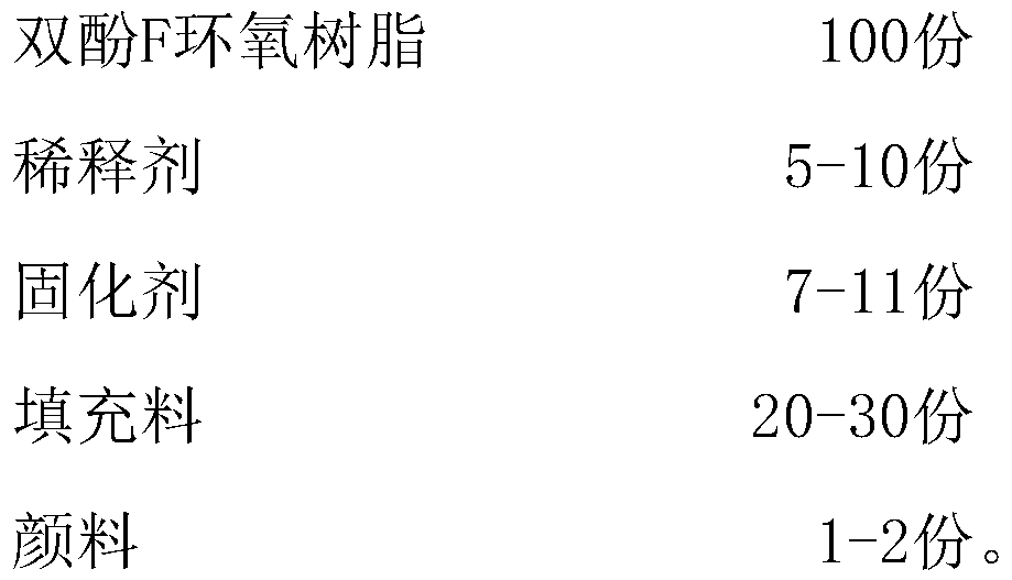
[0031] Wherein, the patch glue includes the raw materials of the following parts by weight:

[0032]

[0033]

[0034] Wherein, the bisphenol F epoxy resin is EPON862.

[0035] Wherein, the diluent is HELOXY8.

[0036] Wherein, the curing agent is composed of EH-4070S and PN23 in a weight ratio of 3:1.

[0037] Wherein, the filler is prepared by ultrasonically dispersing microcr...

Embodiment 2

[0041] A kind of SMT patch technology, comprises the steps:

[0042] (1) Pretreatment: cleaning and drying the PCB board;

[0043] (2) Glue dispensing: use a glue dispenser to apply patch glue to the preset glue dispensing position on the PCB;

[0044] (3) SMT: use a SMT machine to mount the components on the PCB;

[0045] (4) Curing: Send the PCB board into the curing equipment and cure it at 120°C for 2 minutes;

[0046] (5) Reflow soldering: send the PCB board into the reflow soldering furnace for reflow soldering;

[0047] (6) Inspection: check the yield rate of the finished product.

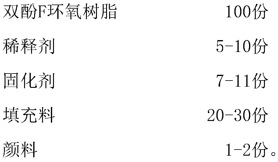
[0048] Wherein, the patch glue includes the raw materials of the following parts by weight:

[0049]

[0050] Wherein, the bisphenol F epoxy resin is EPON862.

[0051] Wherein, the diluent is HELOXY8.

[0052] Wherein, the curing agent is composed of EH-4070S and PN23 in a weight ratio of 5:1.

[0053] Wherein, the filler is prepared by ultrasonically dispersing microcrystalline ce...

Embodiment 3

[0057] A kind of SMT patch technology, comprises the steps:

[0058] (1) Pretreatment: cleaning and drying the PCB board;

[0059] (2) Glue dispensing: use a glue dispenser to apply patch glue to the preset glue dispensing position on the PCB;

[0060] (3) SMT: use a SMT machine to mount the components on the PCB;

[0061] (4) Curing: send the PCB board into the curing equipment, and cure at 110°C for 1 min;

[0062] (5) Reflow soldering: send the PCB board into the reflow soldering furnace for reflow soldering;

[0063] (6) Inspection: check the yield rate of the finished product.

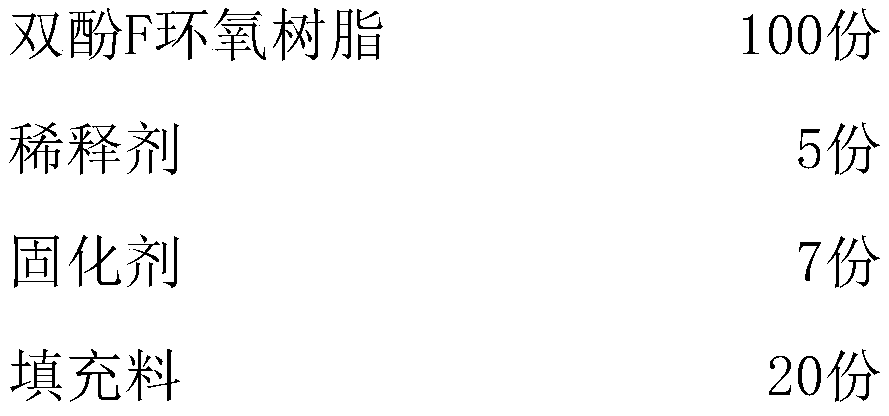
[0064] Wherein, the patch glue includes the raw materials of the following parts by weight:

[0065]

[0066]Wherein, the bisphenol F epoxy resin is EPON862.

[0067] Wherein, the diluent is HELOXY8.

[0068] Wherein, the curing agent is composed of EH-4070S and PN23 in a weight ratio of 4:1.

[0069] Wherein, the filler is prepared by ultrasonically dispersing microcrystalline cellulose...


PUM

PropertyMeasurementUnit
Particle sizeaaaaaaaaaa
Specific surface areaaaaaaaaaaa
Particle sizeaaaaaaaaaa

Abstract

The invention relates to the technical field of surface mounting, in particular to an SMT surface mounting process. The SMT surface mounting process comprises the following steps of: (1) pretreatment:cleaning and drying a PCB; (2) dispensing: coating the preset dispensing position on the PCB with a patch adhesive by using a dispensing machine; (3) chip mounting: mounting the component on the PCBby using a chip mounter; (4) curing: feeding the PCB into curing equipment for curing; (5) reflow soldering: feeding the PCB into a reflow soldering furnace for reflow soldering; and (6) checking: checking the yield of the finished product, wherein the patch adhesive comprises the following raw materials in parts by weight: bisphenol F epoxy resin, a diluent, a curing agent, a filler and a pigment. The chip mounting adhesive adopted in the SMT chip mounting process has the characteristics of the high bonding strength and the high curing speed, low-temperature curing can be achieved at a temperature of 110-130 DEG C, the curing time is only 1-2 minutes, the packaging speed is high, and the production efficiency can be effectively improved.

Description

technical field [0001] The invention relates to the technical field of patching, in particular to an SMT patching process. Background technique [0002] Surface mount technology (SMT) is the fourth generation of electronic assembly technology. Its advantages are high component installation density, small size of electronic products, light weight, high reliability, strong anti-vibration ability, good high-frequency characteristics, and easy automation and integration. Improve production efficiency and reduce costs at the same time. [0003] The SMT placement process in the prior art has defects such as complex process, low product qualification rate, low efficiency, low bonding strength of the placement adhesive, and slow curing speed. Contents of the invention [0004] In order to overcome the disadvantages and deficiencies in the prior art, the object of the present invention is to provide a SMT patching process with high bonding strength and fast curing speed. [0005]...

Claims


Application Information

Patent Timeline
IPC IPC(8): H05K3/34C09J163/00C09J11/04C09J11/08
CPCC09J11/04C09J11/08C09J163/00H05K3/341C08L1/04C08K3/36
Inventor 胡扬扬
Owner 东莞市合权电子有限公司
Why Eureka
Try Eureka