Method for directly growing two-dimensional hexagonal boron nitride on dielectric substrate

A two-dimensional hexagonal and boron nitride technology, applied in the field of material science, can solve the problems of h-BN nucleation difficulties, limited crystal quality, uneven nucleation, etc., achieve good controllability, improve crystal quality, and avoid transfer The effect of the process

Active Publication Date: 2019-12-31
INST OF SEMICONDUCTORS - CHINESE ACAD OF SCI
View PDF5 Cites 4 Cited by
  • Summary
  • Abstract
  • Description
  • Claims
  • Application Information

AI Technical Summary

Problems solved by technology

Due to the lack of catalytic activity of the substrate, the activation energy required for the nucleation of h-BN on the dielectric substrate is relatively high, resulting in difficult nucleation of h-BN on the dielectric substrate, uneven nucleation, limited crystal quality, and small crystal domain size And other issues

Method used


Image

  • Method for directly growing two-dimensional hexagonal boron nitride on dielectric substrate
  • Method for directly growing two-dimensional hexagonal boron nitride on dielectric substrate
  • Method for directly growing two-dimensional hexagonal boron nitride on dielectric substrate

Examples


Embodiment Construction

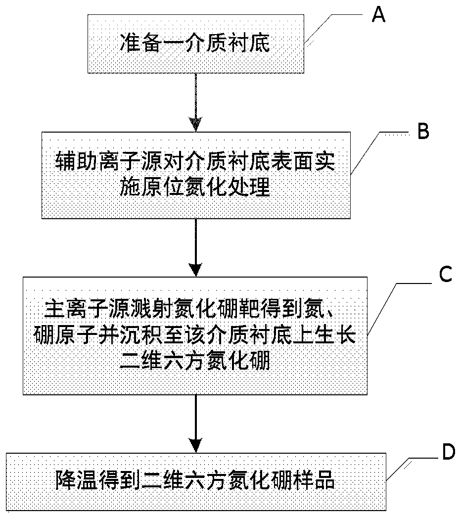
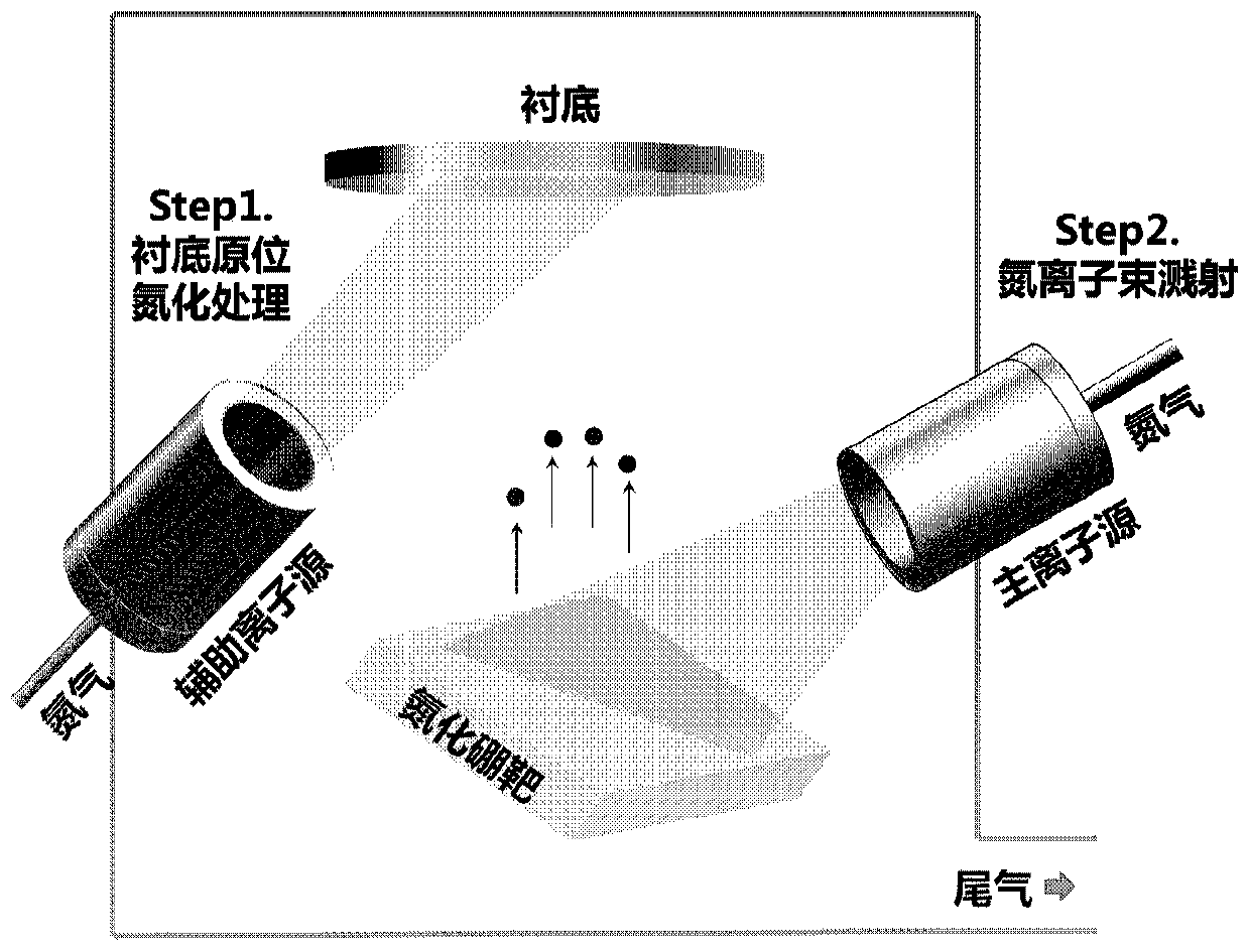
[0037] In order to make the object, technical solution and advantages of the present invention clearer, the present invention will be further described in detail below in conjunction with specific embodiments and with reference to the accompanying drawings.

[0038] The invention adopts ion beam assisted deposition technology to directly grow two-dimensional h-BN on the dielectric substrate, promotes the nucleation of h-BN on the dielectric substrate through in-situ nitriding treatment of the substrate surface by the ion beam, and simultaneously uses nitrogen ions Beam sputtering grows h-BN, provides sufficient nitrogen source, improves the crystal quality of h-BN film, and grows h-BN two-dimensional atomic crystal directly on the dielectric substrate.

[0039] It should be noted that, in the drawings or descriptions of the specification, similar or identical parts all use the same figure numbers. Implementations not shown or described in the accompanying drawings are forms kn...


PUM


Abstract

The invention discloses a method for directly growing two-dimensional hexagonal boron nitride on a dielectric substrate. The method comprises the following steps that the dielectric substrate is prepared, the dielectric substrate is preset in an ion beam sputter deposition chamber, the deposition chamber comprises a boron nitride target, an auxiliary ion source and a main ion source, and the deposition chamber is pre-pumped to a back bottom vacuum degree; the auxiliary ion source performs in-situ nitridation treatment on the surface of the dielectric substrate, the main ion source sputtering the boron nitride target to obtain nitrogen and boron atoms and depositing the nitrogen and the boron atoms onto the dielectric substrate to grow the two-dimensional hexagonal boron nitride; and the sample of the two-dimensional hexagonal boron nitride is obtained by cooling. According to the method for directly growing the two-dimensional hexagonal boron nitride on the dielectric substrate, the crystal quality of hexagonal boron nitride on the dielectric substrate can be improved, the controllability is good, the surface of the prepared thin film is flat, the uniformity is good, and the methodhas very important significance for the application of hexagonal boron nitride optoelectronics.

Description

technical field [0001] The invention relates to the technical field of material science, in particular to a method for directly growing two-dimensional hexagonal boron nitride on a dielectric substrate. Background technique [0002] In recent years, due to its atomic thickness, unique low-dimensional structure, and many excellent physical, chemical and electronic properties, two-dimensional layered materials have aroused people's research upsurge. As the only two-dimensional insulator material, hexagonal boron nitride (h-BN) has become a research hotspot of domestic and foreign scholars in recent years. [0003] h-BN has a layered structure similar to graphene, and the B and N atoms in the layer are sp 2 The hybridization method forms covalent bonds, and the layers are bound together by van der Waals forces. The highly similar crystal structure makes the two have some common characteristics, such as extremely high in-plane elastic modulus, high thermal conductivity, good c...

Claims


Application Information

Patent Timeline
Patent Type & Authority Applications(China)
IPC IPC(8): C23C14/46C23C14/06C23C14/02
CPCC23C14/02C23C14/0647C23C14/3407C23C14/46
Inventor 孟军华张兴旺高孟磊尹志岗吴金良
Owner INST OF SEMICONDUCTORS - CHINESE ACAD OF SCI
Why Eureka
Try Eureka