Ultra-large bandwidth silicon-based waveguide MEMS (Micro-Electro-Mechanical Systems) optical switch

An ultra-large bandwidth, optical switch technology, applied in the direction of optical waveguide light guide, optics, light guide, etc., can solve the problems that cannot meet high-speed and large-capacity communication, and achieve convenient cascading into an optical switch array, simple design principle, and low insertion loss. Effect

Active Publication Date: 2020-01-07
ZHEJIANG UNIV
View PDF20 Cites 5 Cited by
  • Summary
  • Abstract
  • Description
  • Claims
  • Application Information

AI Technical Summary

Problems solved by technology

Traditional switches with electricity as the core can no longer meet the needs of high-speed and large-capacity communications, so people are gradually turning their attention to optical communications

Method used


Image

  • Ultra-large bandwidth silicon-based waveguide MEMS (Micro-Electro-Mechanical Systems) optical switch
  • Ultra-large bandwidth silicon-based waveguide MEMS (Micro-Electro-Mechanical Systems) optical switch
  • Ultra-large bandwidth silicon-based waveguide MEMS (Micro-Electro-Mechanical Systems) optical switch

Examples


Embodiment Construction

[0034] The present invention will be further described below in conjunction with drawings and embodiments.

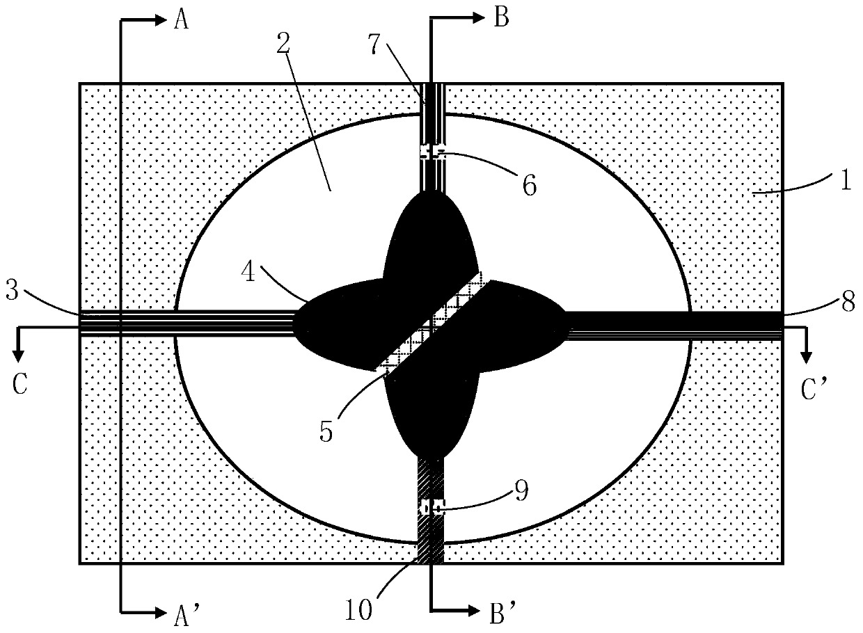
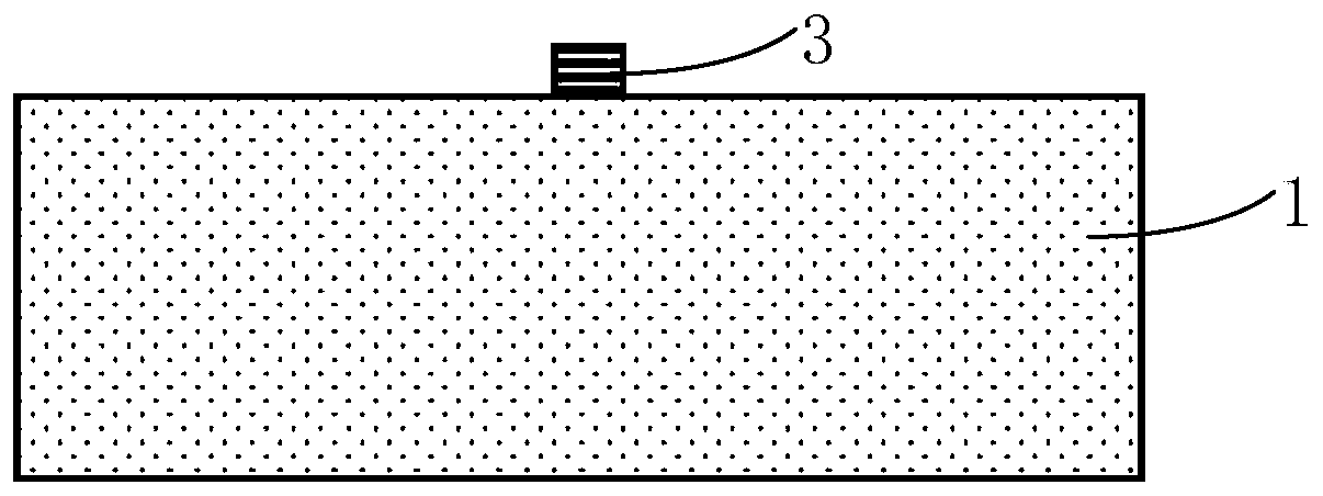
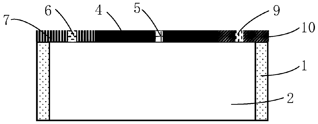
[0035] like figure 1 As shown, the specific implementation of the optical switch includes a silicon dioxide buried oxide layer 1, two input waveguides 3, 10 arranged on the silicon dioxide buried oxide layer 1, a cross waveguide 4 with nano-slopes, and two output waveguides The three parts of 7 and 8; the lower cladding layer of the whole device is made of silicon dioxide to form a silicon dioxide buried oxide layer 1, the upper cladding layer is air, and the lower cladding layer in the vicinity of the crossing waveguide is also air.

[0036] like Figure 1-Figure 4 As shown, the crossing waveguide 4 with nano-slant includes a crossing waveguide body and a nano-sloping groove 5 on the crossing waveguide body. The crossing waveguide body is composed of two elliptical cylinders with the same size and shape. The axial direction is perpendicular to the surface of the sili...


PUM

PropertyMeasurementUnit
thicknessaaaaaaaaaa
thicknessaaaaaaaaaa
refractive indexaaaaaaaaaa

Abstract

The invention discloses an ultra-large bandwidth silicon-based waveguide MEMS (Micro-Electro-Mechanical Systems) optical switch. The optical switch is mainly composed of an input waveguide, a crossedwaveguide with a nano-chute, and an output waveguide; the crossed waveguide consists of two identical orthogonal elliptic cylinders, and four ports of the crossed waveguide respectively extend out ofa single-mode strip-shaped waveguide as an input / output waveguide; the center of a crossed waveguide main body is fully etched with the nano-chute; two symmetric waveguides are etched with a nano-groove; and the crossed waveguide and a lower cladding nearby the nano-groove are through and hollowed out, and the width of the nano-chute is regulated by regulating the voltage applied to the two ends of the crossed waveguide, so that straight-through or total reflection of a light path is realized. According to the ultra-large bandwidth silicon-based waveguide MEMS optical switch provided by the invention, the propagation path of the optical switch is switched by adjusting the voltage applied to the crossed waveguide, the structure is simple, integration and cascade are convenient, and an arraywaveguide optical switch which is miniaturized, low in cost and high in regulation and control speed is expected to be realized.

Description

technical field [0001] The invention relates to an ultra-large bandwidth silicon-based waveguide MEMS optical switch, in particular to an integrated silicon-based waveguide MEMS optical switch capable of controlling the light transmission direction by adding a bias voltage. Background technique [0002] Due to the rapid growth of data traffic and the increasing requirements for reconfigurability and scalability of data center networks, fast optical circuit switches in data center networks have been extensively studied. The traditional switch with electricity as the core can no longer meet the needs of high-speed and large-capacity communication, so people are gradually turning their attention to optical communication. Since the 1990s, optical communication has developed rapidly, and the status of optical interconnection and optical switches, which are key links in optical communication, has naturally become more and more important. [0003] Optical switches are key componen...

Claims


Application Information

Patent Timeline
Patent Type & Authority Applications(China)
IPC IPC(8): G02B6/10G02B6/12G02B6/136G02B26/00G02B26/08
CPCG02B6/107G02B6/12004G02B6/136G02B26/00G02B26/0833G02B2006/12145G02B6/3596G02B6/357G02B6/3506G02B6/3546G02B6/356
Inventor 戴道锌孙仪
Owner ZHEJIANG UNIV
Why Eureka
Try Eureka