Method and system for processing nanocone arrays on silk film using femtosecond laser
A femtosecond laser and nanocone technology, which is applied in the field of femtosecond laser application, can solve the problem of lack of processing nanoscale cone-shaped convex arrays.
- Summary
- Abstract
- Description
- Claims
- Application Information
AI Technical Summary
Problems solved by technology
Method used
Image
Examples
Embodiment 1
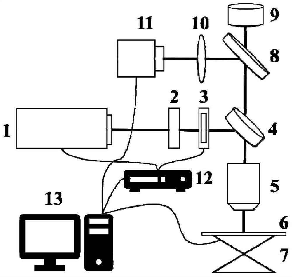
[0053] Adjust the neutral density attenuator 2, and set the energy flux of a single pulse to 6.2J / cm 2 , the moving speed of the translation stage is 800 μm / s, and the scanning interval is 800 nm, and a nanocone array with a diameter of 210 nm, a height of 17.55 nm, and a pitch of 800 nm is obtained on the silk film 6 .
Embodiment 2
[0055] Adjust the neutral density attenuator 2, and set the energy flux of a single pulse to 7J / cm 2 , the moving speed of the translation stage is 1000 μm / s, the scanning interval is 1000 nm, and a nanocone array with a diameter of 320 nm, a height of 44.4 nm, and a pitch of 1000 nm is obtained on the silk film 6 .
Embodiment 3
[0057] Adjust the neutral density attenuator 2 and set the energy flux of a single pulse to 7.7J / cm 2 , the moving speed of the translation stage is 1500 μm / s, the scanning interval is 1500 nm, and a nanocone array with a diameter of 420 nm, a height of 168 nm, and a pitch of 1500 nm is obtained on the silk film 6 .
PUM
| Property | Measurement | Unit |
|---|---|---|
| thickness | aaaaa | aaaaa |
| diameter | aaaaa | aaaaa |
| height | aaaaa | aaaaa |
Abstract
Description
Claims
Application Information
