
Monopole antenna array source for semiconductor process equipment

A monopole antenna and antenna array technology, which is applied in semiconductor/solid-state device manufacturing, resonant antenna, and slender active unit end feeding, etc., can solve the problem that the microwave source cannot meet strict uniformity, and achieve good temperature Effects of controlling, improving processing speed, and increasing yield

Active Publication Date: 2020-01-17
APPLIED MATERIALS INC
View PDF10 Cites 2 Cited by
  • Summary
  • Abstract
  • Description
  • Claims
  • Application Information

AI Technical Summary

Problems solved by technology

However, microwave sources cannot meet the stringent uniformity required to distribute deposition rates or etch rates across an entire workpiece

Method used


Image

  • Monopole antenna array source for semiconductor process equipment
  • Monopole antenna array source for semiconductor process equipment
  • Monopole antenna array source for semiconductor process equipment

Examples


Embodiment Construction

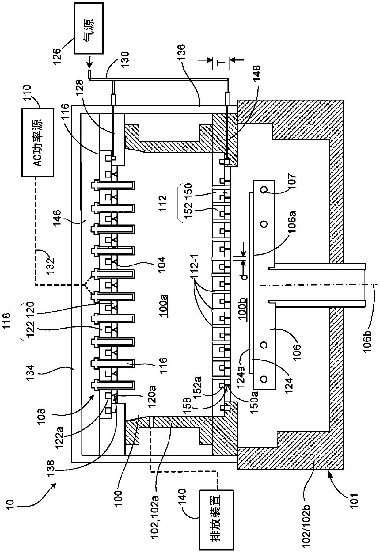
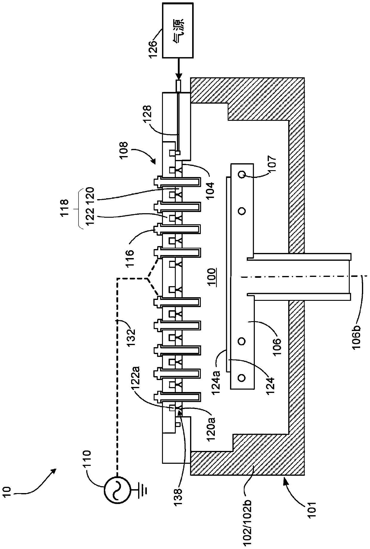
[0042] Processing of workpieces, such as semiconductor wafers, may be performed in plasma reactors. For example, electromagnetic energy such as RF power or microwave (MW) power can be employed to generate a plasma in a chamber to perform plasma-based processing such as plasma-enhanced chemical vapor deposition (PECVD) or plasma Volume Enhanced Reactive Ion Etching (PERIE)). Some processes, such as the deposition of diamond-like carbon (DLC) films, require high plasma ion densities and low plasma ion energies. Higher plasma densities require higher source powers and generally result in shorter deposition times.

[0043] The advantage of microwave sources is that they can produce very high plasma ion densities with less plasma ion energy than other sources (e.g., inductively coupled RF plasma sources or capacitively coupled RF plasma sources). plasma source). Another advantage of microwave plasma sources is the ability to generate plasma over a wide range of chamber pressures...


PUM


Abstract

A plasma reactor includes a chamber body having an interior space that provides a plasma chamber, a gas distribution port to deliver a processing gas to the plasma chamber, a workpiece support to holda workpiece, an antenna array comprising a plurality of monopole antennas extending partially into the plasma chamber, and an AC power source to supply a first AC power to the plurality of monopole antennas.

Description

technical field [0001] This specification relates to wafer processing systems and related methods. Background technique [0002] For example, processing of a workpiece, such as a semiconductor wafer, may be performed using a form of electromagnetic energy, such as RF power or microwave power. For example, power may be employed to generate a plasma for performing plasma-based processes such as plasma-enhanced chemical vapor deposition (PECVD) or plasma-enhanced reactive ion etching (PERIE). Some processes require extremely high plasma ion densities as well as extremely low plasma ion energies. This is true for processes such as the deposition of diamond-like carbon (DLC) films, where the time required to deposit some types of DLC films can be hours, depending on the desired thickness and plasma ion density. Higher plasma densities require higher source powers and generally translate into shorter deposition times. [0003] Microwave sources typically produce very high plasm...

Claims


Application Information

Patent Timeline
IPC IPC(8): H01Q9/40H01L21/3065
CPCC23C16/503H01J37/3211H01J37/32458H01J37/3222H01J37/32449C23C16/26C23C16/45565H01J37/3244H01J37/32724H01L21/67103H01J37/32715H01Q9/40H01L21/3065H05H1/46H05H1/463H05H1/466H05H1/4652C23C16/50H01J2237/3321H01J2237/3341H01L21/02115H01L21/02274H01L21/67017H01J2237/334
Inventor 梁奇伟斯里尼瓦斯·D·内曼尼
Owner APPLIED MATERIALS INC
Features
  • Generate Ideas
  • Intellectual Property
  • Life Sciences
  • Materials
  • Tech Scout
  • Unparalleled Data Quality
  • Higher Quality Content
  • 60% Fewer Hallucinations
Learn More