Lateral double-diffused transistor and manufacturing method of drift region of lateral double-diffused transistor

A technology of lateral double diffusion and manufacturing method, which is applied in the field of manufacturing lateral double diffusion transistors and their drift regions, can solve the problems of low on-resistance, high process cost, less process flow, etc., so as to reduce the process flow and production cost, The effect of low on-resistance

Active Publication Date: 2020-01-24
JOULWATT TECH INC LTD
View PDF6 Cites 1 Cited by
  • Summary
  • Abstract
  • Description
  • Claims
  • Application Information

AI Technical Summary

Problems solved by technology

[0005] In order to provide a method for manufacturing a lateral double-diffused transistor and its drift region that satisfies higher turn-off breakdown voltage and lower on-resistance, and has less process flow, to solve the problem of high process cost in the prior art, In order to reduce the process cost, the present invention provides a method for manufacturing the drift region of the lateral double-diffused transistor

Method used


Image

  • Lateral double-diffused transistor and manufacturing method of drift region of lateral double-diffused transistor
  • Lateral double-diffused transistor and manufacturing method of drift region of lateral double-diffused transistor
  • Lateral double-diffused transistor and manufacturing method of drift region of lateral double-diffused transistor

Examples


Embodiment Construction

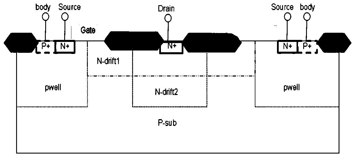
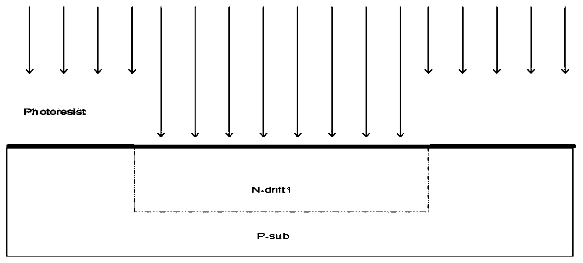
[0051] Preferred embodiments of the present invention will be described in detail below with reference to the accompanying drawings, but the present invention is not limited to these embodiments. The present invention covers any alternatives, modifications, equivalent methods and schemes made within the spirit and scope of the present invention.

[0052] In order to provide the public with a thorough understanding of the present invention, specific details are set forth in the following preferred embodiments of the present invention, but those skilled in the art can fully understand the present invention without the description of these details.

[0053] In the following paragraphs the invention is described more specifically by way of example with reference to the accompanying drawings. It should be noted that all the drawings are in simplified form and use inaccurate scales, which are only used to facilitate and clearly assist the purpose of illustrating the embodiments of t...


PUM

PropertyMeasurementUnit
thicknessaaaaaaaaaa
thicknessaaaaaaaaaa

Abstract

The invention discloses a manufacturing method of the drift region of a lateral double-diffused transistor. According to the method, an adhesive layer and a mask layer are designed; with the adhesivelayer coating a final dielectric layer adopted as a barrier, anisotropic etching is performed on a second dielectric layer, or second dielectric layer and a third dielectric layer, so that the middleregion of the drift region is opened, primary drift region injection is performed; with the adhesive layer or the third dielectric layer adopted as a barrier, isotropic etching is performed on the second dielectric layer, the adhesive layer or the adhesive layer and the third dielectric layer is / or removed, secondary drift region injection is performed with the second dielectric layer adopted as abarrier; between the two times of drift region injection, only one-time photoetching is needed, so that a linear gradient drift region can be formed. With the manufacturing method adopted, technological process and manufacturing cost are reduced, and requirements for higher turn-off breakdown voltage and lower conduction impedance can be met.

Description

technical field [0001] The invention relates to the technical field of electronic devices, in particular to a method for manufacturing a lateral double-diffusion transistor and a drift region thereof. Background technique [0002] Lateral double-diffused transistor (LDMOS) is a short-channel lateral conduction MOSFET, which is fabricated by two diffusions. With the wide application of lateral double-diffused transistors (LDMOS) in integrated circuits, the performance requirements of LDMOS are also getting higher and higher. In order to obtain a higher turn-off breakdown voltage (off-BV) and a lower on-resistance (Rdson), the drift region (drift) is often made into a linear gradient doping. [0003] Such as figure 1 As shown, it is the NLDMOS of the prior art, and its linear gradient drift region is realized by two photolithography and implantation of Ndrift1 and Ndrift2. The process step of above prior art is as figure 2 , 3 As shown in and 4, an oxide layer is first d...

Claims


Application Information

Patent Timeline
Patent Type & Authority Applications(China)
IPC IPC(8): H01L21/336H01L29/78H01L29/06
CPCH01L29/0603H01L29/7816H01L29/66681Y02P70/50
Inventor 韩广涛陆阳周逊伟
Owner JOULWATT TECH INC LTD
Why Eureka
Try Eureka