Semiconductor device and forming method thereof

A semiconductor and device technology, applied in the field of semiconductor devices and their formation, can solve the problems of semiconductor device performance degradation, etc., and achieve the effects of improving uniformity, improving performance, and controlling fin size

Pending Publication Date: 2020-01-24
SEMICON MFG INT (SHANGHAI) CORP +1
View PDF8 Cites 0 Cited by
  • Summary
  • Abstract
  • Description
  • Claims
  • Application Information

AI Technical Summary

Problems solved by technology

[0003] After the existing ion implantation technology performs ion d

Method used


Image

  • Semiconductor device and forming method thereof
  • Semiconductor device and forming method thereof
  • Semiconductor device and forming method thereof

Examples


no. 1 example

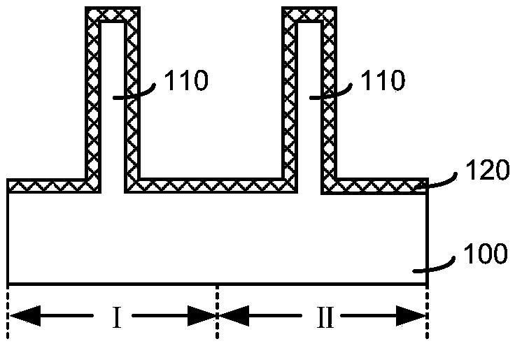
[0045] Please refer to figure 1 , a fin portion 110 is formed on the semiconductor substrate 100 , and a first source doped film 120 is formed on the surface of the semiconductor substrate 100 and the fin portion 110 .

[0046] The semiconductor substrate 100 serves as a process basis for forming semiconductor devices. The material of the semiconductor substrate 100 is polysilicon. In the embodiment of the present invention, the semiconductor substrate 100 also contains other structures, such as: metal plugs, metal connection layers, dielectric layers and other structures, or other semiconductor devices composed of these structures, which are not described here. Specific restrictions.

[0047] In the embodiment of the present invention, the semiconductor substrate 100 includes a first region I and a second region II. The two regions are doped with different types of ions. In the embodiment of the present invention, the first region I and the second region II are respectiv...

no. 2 example

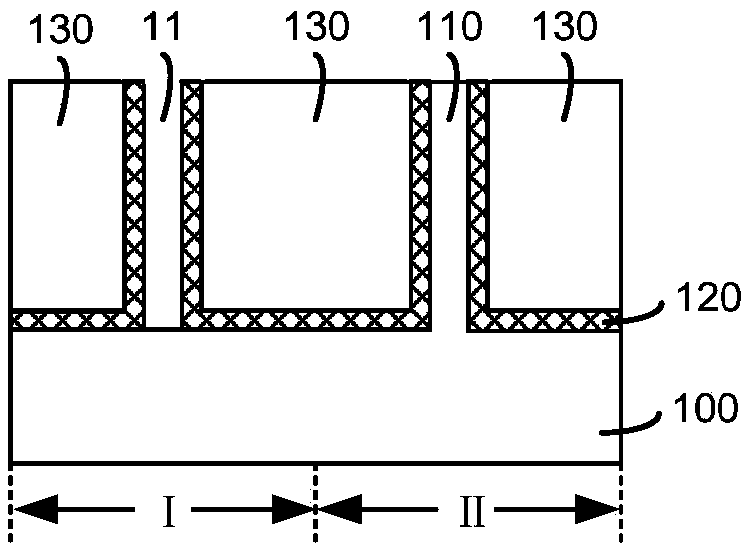
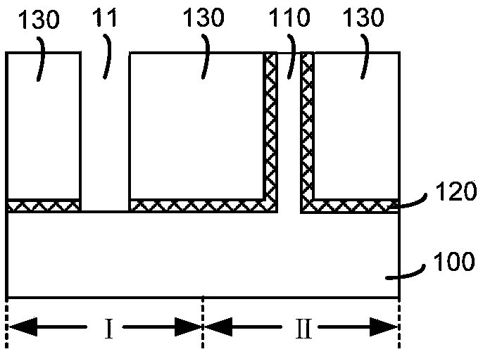
[0099] Please refer to Figure 6-Figure 9 Compared with the first embodiment, the method for forming a semiconductor device according to the second embodiment of the present invention differs in that when the fin above the first region I is removed to form the first groove, the second region is also removed at the same time Ⅱ above the fin to form the second groove. Subsequently, a second replacement fin also needs to be formed in the second groove. Other processes are consistent with the first embodiment.

[0100] Please refer to Figure 6 , the fins above the first region I and the second region II are removed, and the first groove 21 and the second groove 22 are correspondingly formed respectively.

[0101] The formation steps, functions and material selection of the semiconductor substrate 200, the first source-doped thin film 220 and the interlayer dielectric layer 230, as well as the process method for forming the first groove 21 are all consistent with the first embo...


PUM


Abstract

The invention discloses a formation method of a semiconductor device. The method comprises the following steps that: a semiconductor substrate and fin parts are provided, wherein the semiconductor substrate comprise a first region and a second region, and the fin parts are correspondingly arranged on the first region and the second region; a first source doped thin film is formed, wherein the first source doped thin film covers the surfaces of the fin parts; an interlayer dielectric layer is formed between the adjacent fin parts; a part of the interlayer dielectric layer and a part of the first source doped thin film are removed, so that the top surfaces of the fin parts are exposed; the fin part on the first region is removed, so that a first groove can be formed; the first source doped film at two sides of the first groove is removed; a second source doped film covering two side walls of the first groove is formed; a first replacement fin part is formed in the first groove; and the interlayer dielectric layer is treated through an annealing process. After ion diffusion, defects formed on the surface of the fin parts can be avoided.

Description

technical field [0001] The invention relates to the field of semiconductor manufacturing, in particular to a semiconductor device and a forming method thereof. Background technique [0002] As the integration level of integrated circuits increases, the size of semiconductor devices continues to shrink. The Finfet structure has been widely used in devices. At present, after the Finfet is formed, it is generally necessary to perform necessary ion implantation on the fin of the Finfet, so as to realize the function of the semiconductor device or improve the performance of the semiconductor device. [0003] After the existing ion implantation technology performs ion doping on the fin, the performance of the semiconductor device decreases. [0004] Therefore, there is an urgent need for a semiconductor device and a method for forming the semiconductor device that improves the performance of the semiconductor device after ion doping. Contents of the invention [0005] The emb...

Claims


Application Information

Patent Timeline
IPC IPC(8): H01L29/06H01L21/336H01L29/78
CPCH01L29/785H01L29/66795H01L29/0688
Inventor 周飞
Owner SEMICON MFG INT (SHANGHAI) CORP
Why Eureka
Try Eureka