Wide-response spectrum detector based on antimony telluride material and preparation method thereof

A spectral detector, antimony telluride technology, applied in semiconductor devices, final product manufacturing, sustainable manufacturing/processing, etc., can solve the problems of not giving the photoelectric response performance and detection spectrum range, and shorten the annealing time , Reduce the preparation cost and improve the performance of the device

Inactive Publication Date: 2020-01-24
KUNMING INST OF PHYSICS
View PDF3 Cites 7 Cited by
  • Summary
  • Abstract
  • Description
  • Claims
  • Application Information

AI Technical Summary

Problems solved by technology

In addition, although the patent US10096736B1 mentioned the Sb-based 2 Te 3 / Si heterojunction photodetector, but did not give its photoelectric response performance and detection spectrum range

Method used


Image

  • Wide-response spectrum detector based on antimony telluride material and preparation method thereof
  • Wide-response spectrum detector based on antimony telluride material and preparation method thereof
  • Wide-response spectrum detector based on antimony telluride material and preparation method thereof

Examples


Embodiment 1

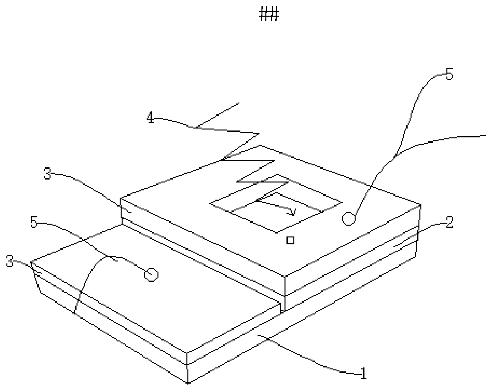
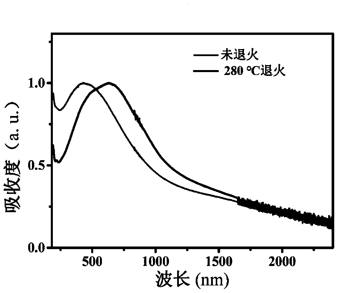
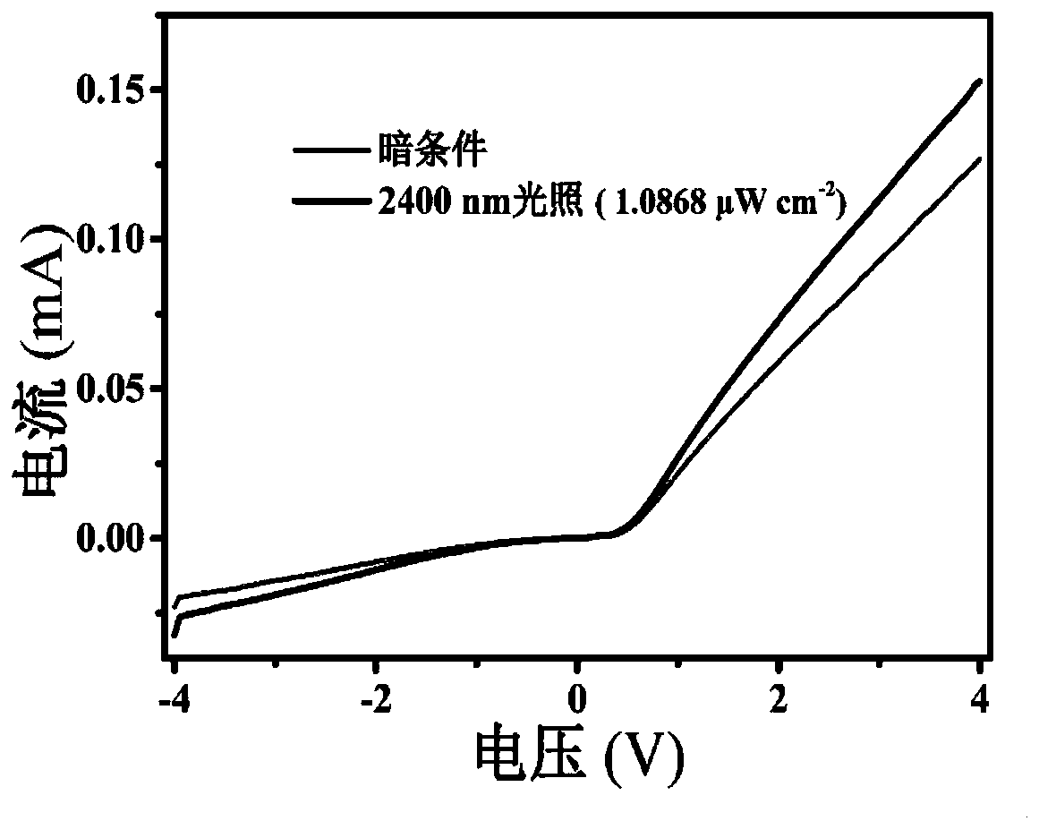
[0019] Embodiment 1: antimony telluride-based wide response spectrum detector, its spectral response layer is a topological insulator material Sb 2 Te 3 Thin film, the substrate is n-Si heterojunction substrate.

[0020] From bottom to top, the detectors are n-Si substrate 1, Sb 2 Te 3 Thin film layer 2, Al electrode layer 3.

[0021] The preparation steps of the detector are as follows:

[0022] S1, clean the substrate: cut a 2.5cm×5cm n-Si substrate 1, put it into the solution of ammonia water:hydrogen peroxide:deionized water ratio of 1:1:3, under the condition of 80°C, Heating for 30min to clean the n-Si substrate.

[0023] S2, Sb 2 Te 3 Thin-film layer sputtering: Put the cleaned n-Si substrate on the sample stage in the magnetron sputtering equipment, and cover half of the area with a clean mold, then turn on the magnetron sputtering equipment, vacuumize, wait for Vacuum to 7.5×10 - 4 After the Pa is below, pre-sputtering is performed first. After the pre-sputt...


PUM


Abstract

Provided are a wide-response spectrum detector based on an antimony telluride material and a preparation method thereof. The invention relates to the technical field of photoelectric, and particularlyrelates to a photoelectric detector with high detection rate, high response rate and wide response spectrum based on a topological insulator material Sb2Te3 and n-Si and a preparation method thereof.According to the wide-response spectrum detector based on an antimony telluride material, a spectrum response layer is a topological insulator material Sb2Te3 film, and a substrate is an n-Si heterojunction substrate. The preparation process comprises the steps of substrate cleaning, Sb2Te3 film sputtering, annealing and Al electrode plating. Compared with the prior art, the preparation of a high-performance wide-spectrum prototype photoelectric detector with a response range of 250-2400nm is realized, and the detector can respond to 250nm in the ultraviolet band and respond to 2400nm in theinfrared band. The preparation period is short, and the device performance is good.

Description

technical field [0001] The invention relates to the field of optoelectronic technology, in particular to a topological insulator material based on Sb 2 Te 3 A photodetector preparation method with high detection rate, high responsivity and wide response spectrum of n-Si. Background technique [0002] Topological insulators are a new research hotspot in the field of materials in recent years. As a new quantum state of matter, topological insulators have many novel physical properties. Topological insulators are completely different from metals and insulators in the traditional sense. The interior of a topological insulator is an insulator with an energy gap, while the surface is a metal surface state with no energy gap protected by time-reversal symmetry. This unique band structure makes it very suitable for developing broadband detectors. In the field of photodetection, current research mainly focuses on the Bi 2 Se 3 family of topological insulator materials, such as B...

Claims


Application Information

Patent Timeline
IPC IPC(8): H01L31/032H01L31/102H01L31/18
CPCH01L31/032H01L31/102H01L31/18Y02P70/50
Inventor 唐利斌张玉平邢一山赵鹏舒恂
Owner KUNMING INST OF PHYSICS
Why Eureka
Try Eureka