

Growth method of light emitting diode and light emitting diode
A technology of light-emitting diodes and growth methods, applied in the field of semiconductor lighting, can solve problems such as uneven LED light emission, uneven In distribution, and In precipitation, and achieve the effects of improving luminous brightness, improving electrostatic discharge ESD, and reducing driving voltage
- Summary
- Abstract
- Description
- Claims
- Application Information
AI Technical Summary
Problems solved by technology
Method used
Image

Examples
Embodiment 1
[0055] The light-emitting diode of this embodiment is obtained according to the following growth method:
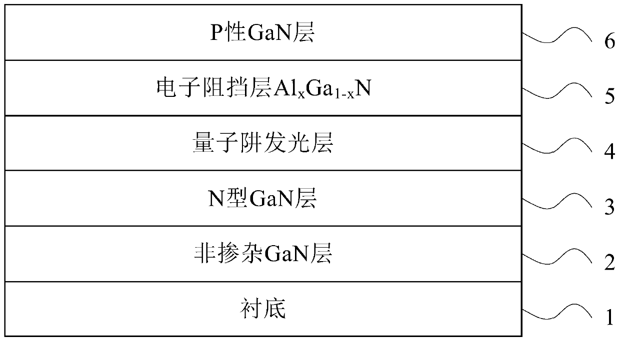
[0056] 1. Put the sapphire (Pattern Sapphire Substrate, PSS for short) substrate into the reaction chamber, N 2 :H 2 : NH 3 The flow rate ratio is (0:120:0) liters per minute (Standard Liter per Minute, referred to as SLM), the pressure of the reaction chamber is 200 Torr (Torr), the temperature is raised to 1080 ° C, stabilized for 300 seconds, and the substrate Perform high temperature purification;
[0057] 2. Raise the temperature to 1050°C, N 2 :H 2 : NH 3 The flow rate ratio is (75:150:56) SLM, the pressure of the reaction chamber is controlled at 450Torr, the speed of the carrier plate is controlled at 1100 rpm, and a non-doped gallium nitride U-GaN layer with a thickness of 1200nm is grown;
[0058] 3. Keep the temperature at 1050°C, N 2 :H 2 : NH 3 The flow rate ratio is (64:120:50) SLM, the pressure of the reaction chamber is controlled at 200Torr, and ...
Embodiment 2
[0065] 1. Put the sapphire (Pattern Sapphire Substrate, PSS for short) substrate into the reaction chamber, N 2 :H 2 : NH 3 The flow rate ratio is (0:120:0) liters per minute (Standard Liter per Minute, referred to as SLM), the pressure of the reaction chamber is 200 Torr (Torr), the temperature is raised to 1080 ° C, stabilized for 300 seconds, and the substrate Perform high temperature purification;
[0066] 2. Raise the temperature to 1050°C, N 2 :H 2 : NH 3 The flow rate ratio is (75:150:56) SLM, the pressure of the reaction chamber is controlled at 450Torr, the speed of the carrier plate is controlled at 1100 rpm, and a non-doped gallium nitride U-GaN layer with a thickness of 1200nm is grown;
[0067] 3. Keep the temperature at 1050°C, N 2 :H 2 : NH 3 The flow rate ratio is (64:120:50) SLM, the pressure of the reaction chamber is controlled at 200Torr, and the N-type gallium nitride N-GaN layer with a thickness of 1000nm is grown;
[0068] 4. Control the tempera...
Embodiment 3
[0074] 1. Put the sapphire (Pattern Sapphire Substrate, PSS for short) substrate into the reaction chamber, N 2 :H 2 : NH 3 The flow rate ratio is (0:120:0) liters per minute (Standard Liter per Minute, referred to as SLM), the pressure of the reaction chamber is 200 Torr (Torr), the temperature is raised to 1080 ° C, stabilized for 300 seconds, and the substrate Perform high temperature purification;
[0075] 2. Raise the temperature to 1050°C, N 2 :H 2 : NH 3 The flow rate ratio is (75:150:56) SLM, the pressure of the reaction chamber is controlled at 450Torr, the speed of the carrier plate is controlled at 1100 rpm, and a non-doped gallium nitride U-GaN layer with a thickness of 1200nm is grown;
[0076] 3. Keep the temperature at 1050°C, N 2 :H 2 : NH 3 The flow rate ratio is (64:120:50) SLM, the pressure of the reaction chamber is controlled at 200Torr, and the N-type gallium nitride N-GaN layer with a thickness of 1000nm is grown;
[0077] 4. Control the tempera...
PUM
| Property | Measurement | Unit |
|---|---|---|
| Thickness | aaaaa | aaaaa |
| Thickness | aaaaa | aaaaa |
| Thickness | aaaaa | aaaaa |
Abstract
Description
Claims
Application Information