Absolute spectral response calibration system and calibration method for optical charge-coupled device
A charge-coupled device and spectral response technology, which is applied in the fields of testing optical performance and spectrum investigation, can solve the problems of complex calibration system structure and system composition, impact on the accuracy of calibration results, and limitations in popularity, and achieves a simple, efficient, and shortened calibration method. The effect of calibrating time and improving experimental efficiency
- Summary
- Abstract
- Description
- Claims
- Application Information
AI Technical Summary
Problems solved by technology
Method used
Image
Examples
Embodiment 1
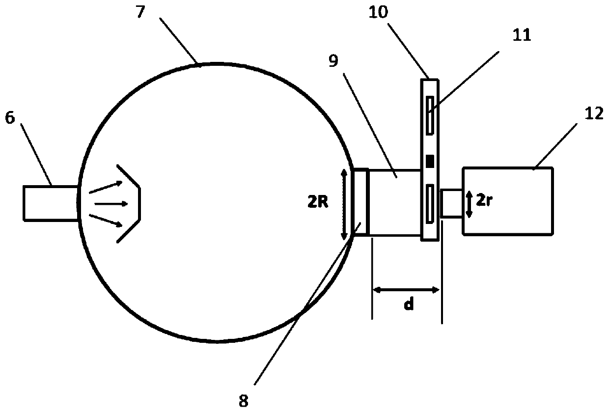
[0040] like figure 2 As shown, an optical charge-coupled device absolute spectral response calibration system sequentially includes a standard integrating sphere light source, a bandpass filter wheel and a CCD12 to be calibrated along the light transmission path.
[0041] Specifically, the standard integrating sphere light source includes an integrating sphere 7 and a standard light source 6, the light emitted by the standard light source 6 enters the integrating sphere 7 through the entrance on the integrating sphere 7, and the light passes through the light outlet 8 after being diffusely reflected inside the integrating sphere 7 shoot. The standard light source 6 is a stable and continuous visible light source, such as a bromine tungsten lamp, whose spectral range covers the visible light band between 380nm and 780nm, so as to be used for calibration of the energy spectral response of the CCD12 to be calibrated at different wavelengths. At the same time, the standard light...
Embodiment 2
[0048] The same part of this embodiment and Embodiment 1 will not be described again, the difference is:
[0049] The standard light source 6 uses a stable and continuous visible light source as input, the brightness temperature is 3000K, and the spectral range covers the range of 350nm to 800nm. The diameter of the light outlet 8 of the integrating sphere is 5cm, and the power density near the light outlet 8 is 1.5w / cm 2 . According to the spectral distribution, the spectral power density distribution at the position of the light outlet 8 can be obtained, such as Image 6 shown. Filter 15 is calibrated with 6 channels, the center wavelength and bandwidth are selected as 400±40nm, 470±40nm, 540±40nm, 610±40nm, 680±40nm, 750±40nm, the transmittance curve of filter 15 is as follows Figure 7 shown.
[0050] During calibration, each channel maintains the same exposure time, and the filter wheel 11 is rotated so that the centers of the filters 15 are aligned with the centers o...
Embodiment 3
[0052] The same part of this embodiment and embodiment two will not be repeated, the difference is:
[0053] The central wavelength and bandwidth of the filter 15 are respectively 400±20nm, 470±50nm, 540±30nm, 610±40nm, 680±30nm, 750±30nm, and the transmittance curve of the filter 15 is as follows Figure 10 shown.
[0054] Obtain the spectral response function curve of the CCD12 to be calibrated according to the spectral analysis method, such as Figure 11 As shown, the black solid line is the ideal spectral response, and the black dashed line is the system spectral response after the system inverse solution. Depend on Figure 11 It can be seen that the reduction degree of the spectral response is very high, and the data reduction rate of each channel can be approximately 1. At the same time, the relative error of the spectral analysis result of the system after considering the random error of the system is 0.82%.
PUM
 Abstract
Description
Claims
Application Information


