Sunken spiral inductor structure and fabrication method thereof

A technology of spiral inductors and manufacturing methods, which is applied in the manufacture of inductors/transformers/magnets, inductors, printed inductors, etc., and can solve problems such as high cost, small inductance value, and power loss

Active Publication Date: 2020-02-07
福建省福联集成电路有限公司
View PDF4 Cites 3 Cited by
  • Summary
  • Abstract
  • Description
  • Claims
  • Application Information

AI Technical Summary

Problems solved by technology

[0003] Therefore, it is necessary to provide a concave spiral inductor structure and its manufacturing method to solve the problems of large occupied area, high cost, small inductance value, power loss, and power integration in the planar inductor structure during chip manufacturing and use.

Method used


Image

  • Sunken spiral inductor structure and fabrication method thereof
  • Sunken spiral inductor structure and fabrication method thereof
  • Sunken spiral inductor structure and fabrication method thereof

Examples


Embodiment Construction

[0049] In order to explain in detail the technical content, structural features, achieved goals and effects of the technical solution, the following will be described in detail in conjunction with specific embodiments and accompanying drawings.

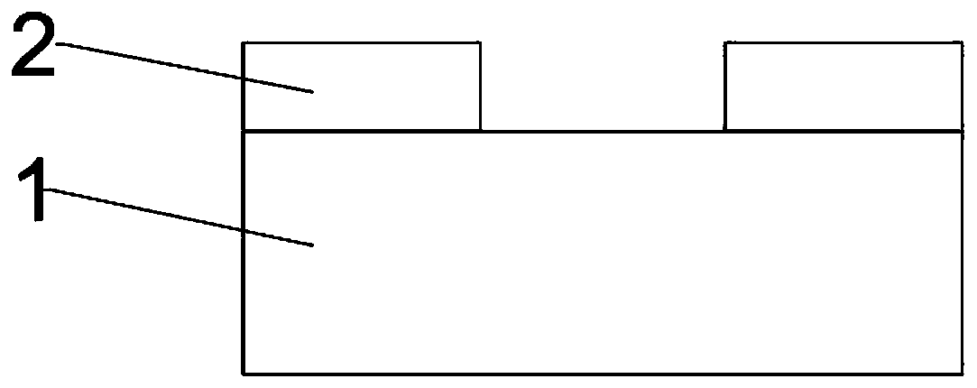
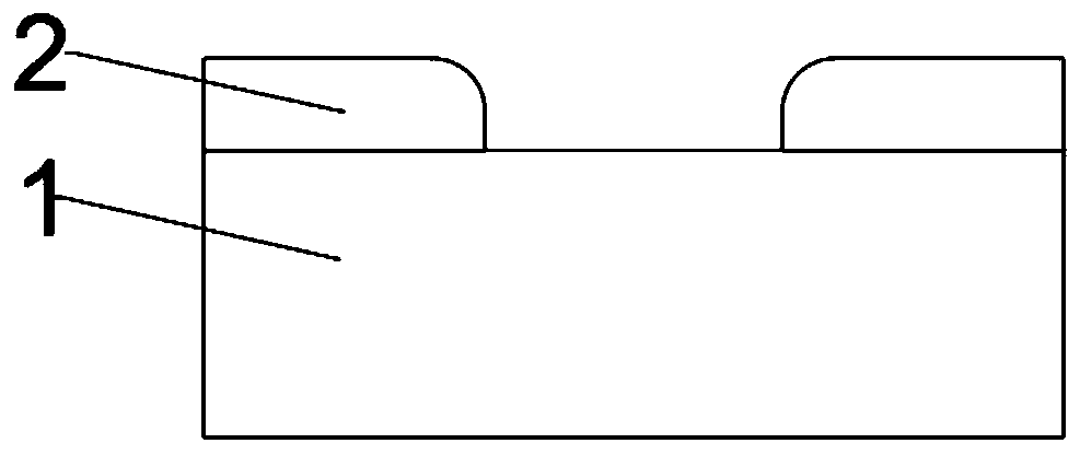
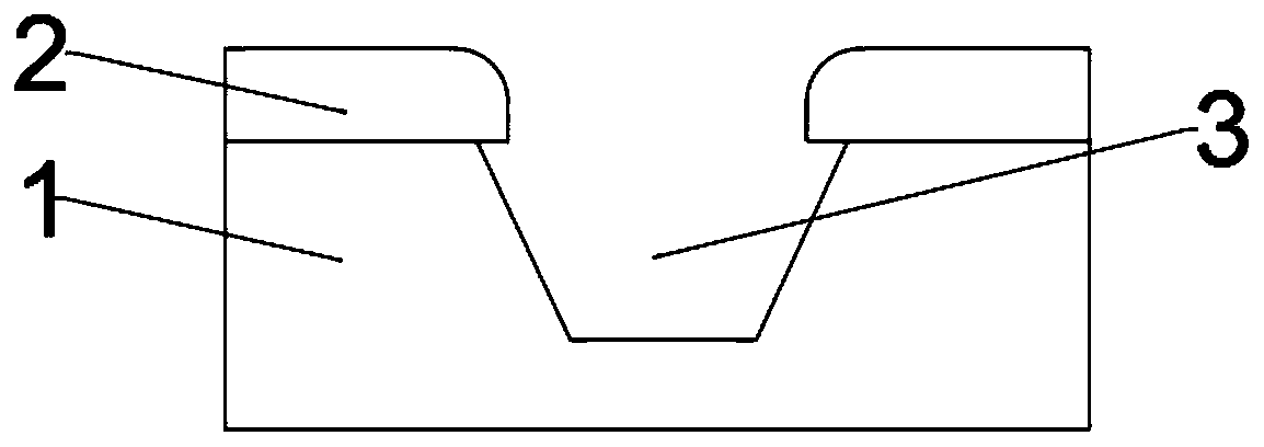
[0050] see Figure 1 to Figure 14, this embodiment provides a method for manufacturing a recessed spiral inductor structure, which can be manufactured on a semiconductor substrate 1 . The method includes the following steps: coating the first photoresist 2, exposing and developing at the groove 3 to be formed, and making an opening above the groove 3 to be formed. A groove 3 is etched on the semiconductor substrate 1, and the redundant first photoresist 2 on the semiconductor substrate 1 is removed. Coating the second photoresist 4 , exposing and developing at the groove 3 to make a window larger than the diameter of the groove 3 . Metal coating is then performed, and metal is sputtered in the groove 3 to form a bottom metal coil 5 ...


PUM


Abstract

The invention discloses a sunken spiral inductor structure and a fabrication method thereof. The method comprises the following steps of etching a groove in a semiconductor substrate, depositing a bottom-layer metal coil and a top-layer metal coil, and forming the sunken spiral inductor structure. By the design of changing the top-layer metal coil and the bottom-layer metal coil of an inductor tobe air gaps and taking air as a medium, a Q (quality factor) value is substantially improved, meanwhile, the self-resonant frequency is also improved, so that an inductance value is improved, the power loss is reduced, and the performance of the inductor is better. On the basis of the sunken spiral inductor structure, the parasitic capacitance on the semiconductor substrate can be greatly reduced.

Description

technical field [0001] The invention relates to the field of chips, in particular to a recessed spiral inductor structure and a manufacturing method thereof. Background technique [0002] Inductors play an important role in the manufacture of semiconductor circuits, and nowadays, with the progress of society, many fields are inseparable from semiconductor circuits. For example, the current 5G wireless communication and GPS have higher and higher requirements for high-performance radio frequency circuits and passive devices. Among them, the Q (quality factor) value of the inductor has an important impact on the performance of high-performance radio frequency circuits. Q (quality factor ) The larger the value, the higher the inductance value, which means better performance. At present, the closest existing technology for semiconductor circuit inductance is mainly a planar spiral structure. In the early stage, because the inductance value required by the power device is relati...

Claims


Application Information

Patent Timeline
Patent Type & Authority Applications(China)
IPC IPC(8): H01L23/64H01L49/02H01F17/00H01F27/28H01F41/04
CPCH01L28/10H01L23/645H01F41/041H01F17/0006H01F27/2804H01F2017/0086H01F2017/0073
Inventor 徐智文温春兰
Owner 福建省福联集成电路有限公司
Why Eureka
Try Eureka