Capacitor and manufacturing method thereof

A capacitor and electrode technology, applied in the field of capacitors, can solve the problems of high price and high cost of silicon wafers, and achieve the effect of reducing unit processing cost and cost

Pending Publication Date: 2020-02-11
SHENZHEN GOODIX TECH CO LTD
View PDF4 Cites 16 Cited by
  • Summary
  • Abstract
  • Description
  • Claims
  • Application Information

AI Technical Summary

Problems solved by technology

However, due to the high price of silicon wafers, the cost of trenched silicon capacitors based on silicon wafers is relative

Method used


Image

  • Capacitor and manufacturing method thereof
  • Capacitor and manufacturing method thereof
  • Capacitor and manufacturing method thereof

Examples


Embodiment 1

[0304] Step 1: Select fused silica glass as the non-semiconductor substrate.

[0305] Step 2: using a plasma enhanced chemical vapor deposition (Plasma Enhanced Chemical Vapor Deposition, PECVD) process to deposit a 10 micron amorphous silicon layer on the non-semiconductor substrate as the first semiconductor layer.

[0306] Step 3: First, use patterning techniques such as photolithography, nanoimprinting, and laser direct writing to form a patterned mask layer on the upper surface of the first semiconductor layer, and then use a deep silicon etching process to form a second mask layer on the first semiconductor layer. A trench array.

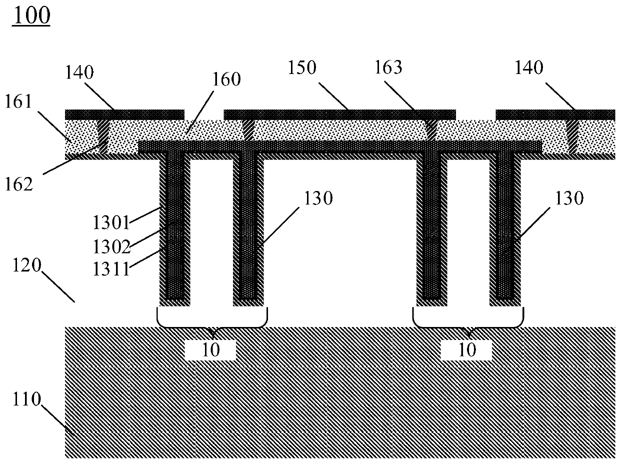
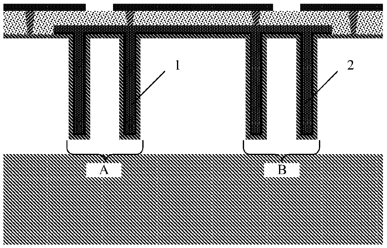
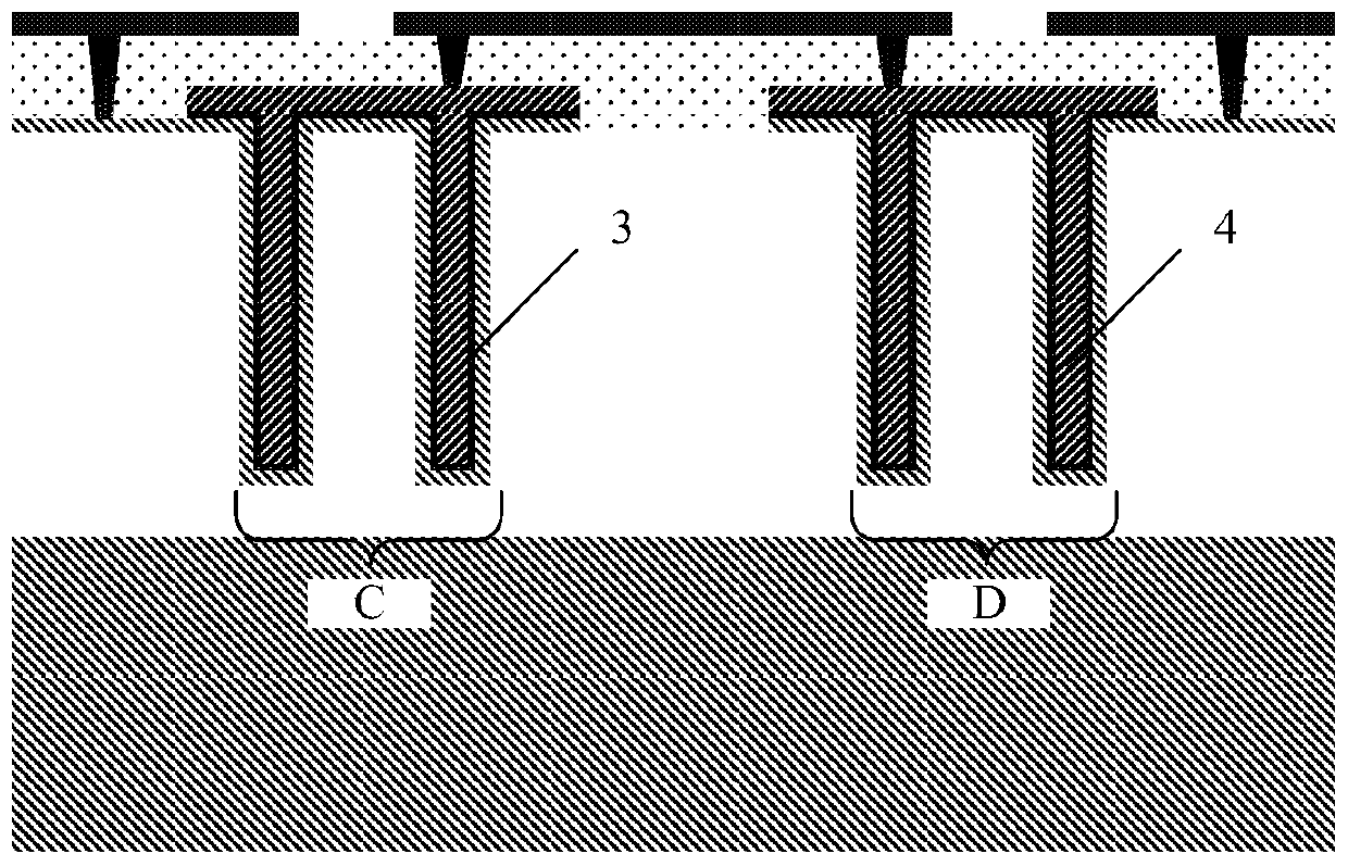
[0307] Step 4: Deposit a layer of TiN as the first conductive layer on the trench sidewalls in the first trench array by using the ALD process. If the non-semiconductor substrate is resistant to high temperature, such as fused silica, this step can also use a doping process to form a low-resistivity conductive layer on the sidewalls of the tr...

Embodiment 2

[0314] Step 1: Select fused silica glass as the non-semiconductor substrate.

[0315] Step 2: Deposit a 10-micron amorphous silicon layer on the non-semiconductor substrate by PECVD process as the first semiconductor layer.

[0316] Step 3: First, use patterning techniques such as photolithography, nanoimprinting, and laser direct writing to form a mask layer with a pattern on the upper surface of the first semiconductor layer, and then use a deep silicon etching process to form a patterned mask layer on the first semiconductor layer. A first trench array is formed.

[0317] Step 4: Deposit a layer of TiN as the first conductive layer on the trench sidewalls in the first trench array by using the ALD process. If the non-semiconductor substrate is resistant to high temperature, such as fused silica, this step can also use a doping process to form a low-resistivity conductive layer on the sidewalls of the trenches in the first trench array.

[0318] Step 5: Using the ALD proce...


PUM


Abstract

The embodiment of the invention provides a capacitor and a manufacturing method thereof. The capacitor comprises a non-semiconductor substrate; a first semiconductor layer arranged above the non-semiconductor substrate, at least one first trench array being formed in the first semiconductor layer; at least one first laminated structure arranged above the first semiconductor layer and filling the at least one first trench array, the first laminated structure comprising N conductive layers and M dielectric layers, the N conductive layers and the M dielectric layers forming a structure in which the conductive layers and the dielectric layers are adjacent to each other, and N and M being positive integers; at least one first external electrode electrically connected to all odd conductive layers in the N conductive layers; and at least one second external electrode electrically connected to all even conductive layers in the N conductive layers.

Description

technical field [0001] This application relates to the field of capacitors, and more particularly, to capacitors and methods of making them. Background technique [0002] Capacitors can play the role of bypass, filtering, decoupling, etc. in the circuit, and are an indispensable part to ensure the normal operation of the circuit. With the continuous development of modern electronic systems towards multi-function, high integration, low power consumption, and miniaturization, compared with traditional multi-layer ceramic capacitors (Multi-layer Ceramic Capacitors, MLCC), trenched silicon based on silicon wafers Capacitors can reduce the volume of the capacitor and increase the capacitance density. However, due to the high price of silicon wafers, the cost of trench silicon capacitors prepared based on silicon wafers is relatively high. How to prepare low-cost, small-volume, high-capacity capacitors has become an urgent technical problem to be solved. Contents of the inventi...

Claims


Application Information

Patent Timeline
IPC IPC(8): H01L23/64H01L49/00H01L21/82
CPCH01L28/40H01L28/90H01L21/82H10N99/00
Inventor 陆斌沈健
Owner SHENZHEN GOODIX TECH CO LTD
Why Eureka
Try Eureka