An optical power splitter based on three-coupled waveguides with transverse magnetic mode cutoff and transverse electric mode equalization

A technology of coupling waveguide and optical power splitter, applied in the field of integrated optics, can solve the problems of high insertion loss, high ohmic loss, unfavorable PIC dense integration, etc., and achieve the effect of low insertion loss, high ohmic loss and compact structure

Active Publication Date: 2020-11-03
SOUTHEAST UNIV
View PDF8 Cites 0 Cited by
  • Summary
  • Abstract
  • Description
  • Claims
  • Application Information

AI Technical Summary

Problems solved by technology

However, since the introduction of metal materials also brings high ohmic loss, the insertion loss of the mode analyzer based on the single structure of the hybrid plasmonic waveguide is generally high, which is not conducive to the application of this device in high-performance photonic circuits.
In addition, the cascading of pre-mode analyzers and post-power dividers is not conducive to the dense integration of PICs

Method used


Image

  • An optical power splitter based on three-coupled waveguides with transverse magnetic mode cutoff and transverse electric mode equalization
  • An optical power splitter based on three-coupled waveguides with transverse magnetic mode cutoff and transverse electric mode equalization
  • An optical power splitter based on three-coupled waveguides with transverse magnetic mode cutoff and transverse electric mode equalization

Examples


Embodiment Construction

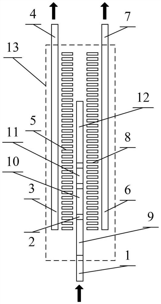
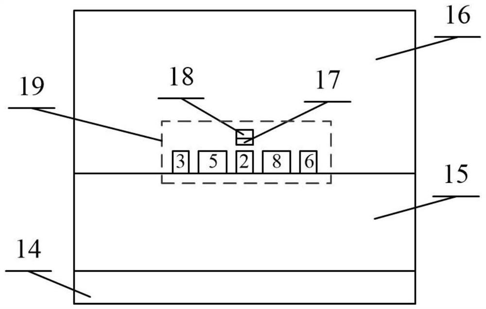
[0029] like figure 1 and image 3 As shown, the optical power splitter consists of a silicon-based substrate 14, a buried oxide layer 15, an optical power sub-component 19 and an upper cladding layer 16 from bottom to top, wherein the buried oxide layer 15 is grown on the upper surface of the silicon-based substrate 14 , the upper cladding layer 16 covers the upper surface of the buried oxide layer 15 , and the optical power component 19 grows horizontally on the upper surface of the buried oxide layer 15 and is covered by the upper cladding layer 16 .

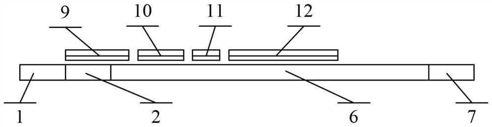
[0030]The optical power component 19 includes a lower layer input channel 1, a lower layer middle channel through channel 2, a lower layer left channel through channel 3, a lower layer left output channel 4, a lower layer left subwavelength grating channel 5, a lower layer right channel through channel 6, and a lower layer right channel Output channel 7, lower right sub-wavelength grating channel 8, upper middle direct channe...


PUM

PropertyMeasurementUnit
thicknessaaaaaaaaaa

Abstract

The invention discloses an optical power divider based on three-coupling-waveguide transverse magnetic mode cutoff and transverse electric mode uniform distribution. The optical power divider comprises a silicon-based substrate, a buried oxide layer, a power division part and an upper cladding layer in sequence from bottom to top, wherein the buried oxide layer is grown on the upper surface of thesilicon-based substrate, the upper cladding layer covers the upper surface of the buried oxide layer, and the optical power division part is horizontally grown on the upper surface of the buried oxide layer and covered by the upper cladding layer. According to the optical power divider, the insertion loss of the optical power divider can be greatly reduced, the extinction ratio of the optical power divider is increased, the size of the optical power divider is reduced, and the manufacturing difficulty of the optical power divider is lowered.

Description

technical field [0001] The invention relates to the technical field of integrated optics, in particular to an optical power splitter based on three-coupling waveguides with transverse magnetic mode cutoff and transverse electric mode equalization. Background technique [0002] In recent years, the silicon-on-insulator (SOI) material system has attracted much attention as a fabrication platform for integrated photonic circuits (PICs). In PIC, the optical power splitter is the key device to achieve power distribution between channels, but the refractive index difference between the cladding layer and the core layer in the SOI material is large, which is prone to polarization-related problems, including polarization mode dispersion and polarization-dependent gain. Therefore, polarization control of power distribution becomes essential in PICs. The usual solution is to first use a mode analyzer to eliminate unwanted polarized light, and then cascade a power splitter. Generally...

Claims


Application Information

Patent Timeline
Patent Type & Authority Patents(China)
IPC IPC(8): G02B6/122
CPCG02B6/122G02B6/1226G02B2006/12038G02B2006/12085G02B2006/12152
Inventor 肖金标陈禹飞
Owner SOUTHEAST UNIV
Why Eureka
Try Eureka