Circuit and method for detecting characteristics of transistor in pixel region of LTPSAMOLED display substrate

A technology for detecting transistors and transistor characteristics, applied to static indicators, instruments, etc., can solve the problems of insufficient accuracy, low success rate, and large fluctuation of test results, so as to optimize the reset effect and improve the effect of flicker and afterimage

Active Publication Date: 2020-02-21
BOE TECH GRP CO LTD +1
View PDF22 Cites 5 Cited by
  • Summary
  • Abstract
  • Description
  • Claims
  • Application Information

AI Technical Summary

Problems solved by technology

[0004]But for the first method, the success rate is extremely low due to the difficulty in controlling the corrosion accuracy of the composite film layer and the mechanical grinding ac...

Method used


Image

  • Circuit and method for detecting characteristics of transistor in pixel region of LTPSAMOLED display substrate
  • Circuit and method for detecting characteristics of transistor in pixel region of LTPSAMOLED display substrate
  • Circuit and method for detecting characteristics of transistor in pixel region of LTPSAMOLED display substrate

Examples


Embodiment 1

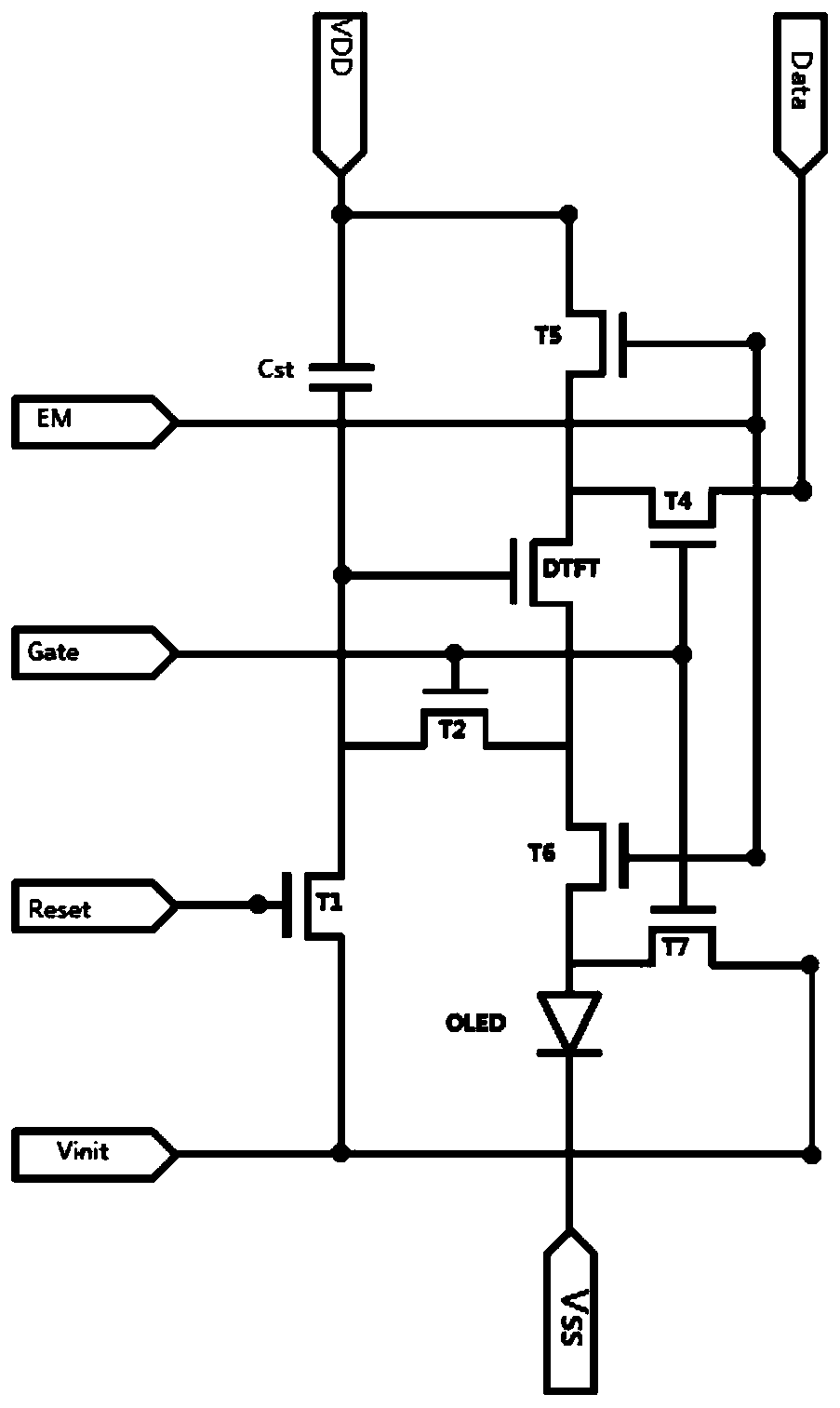
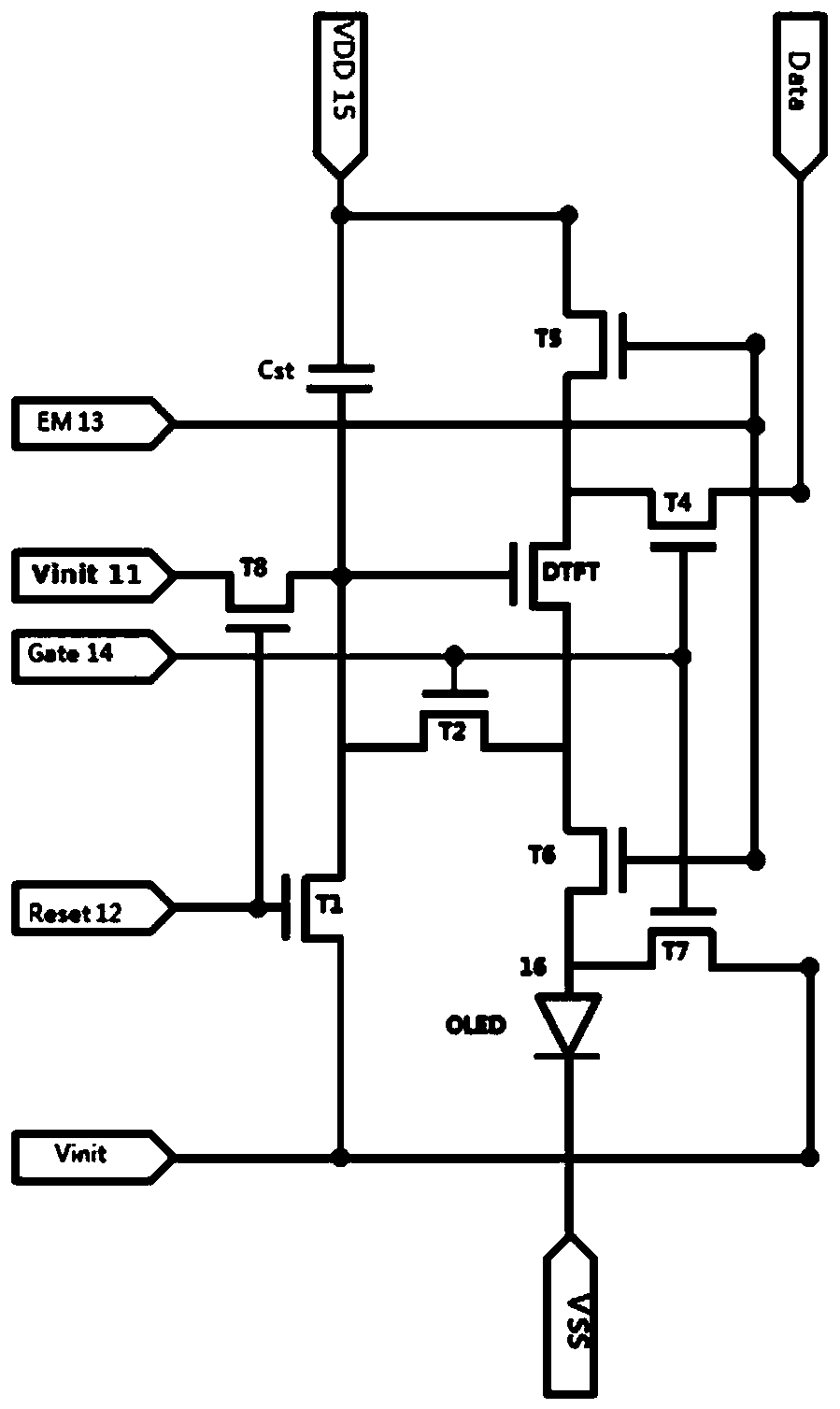
[0051] The following takes 7T1C as an example to illustrate the specific circuit structure and working process of the solution of Embodiment 1 of the present invention.

[0052] Such as figure 2 As shown, the initialization module includes a first transistor T1 and a seventh transistor T7, wherein the gate of the first transistor T1 is connected to a reset signal (Gate n-1 ), the first pole of the first transistor T1 is connected to the second pole of the detection transistor T8, the gate of the driving transistor DTFT and the first pole of the storage capacitor. The second electrode of the first transistor T1 is connected to the reset voltage Vinit. The gate of the seventh transistor T7 is connected to the scan signal Gate n , the first pole is connected to the anode of the electroluminescence element OLED, and the second pole is connected to the reset voltage Vinit.

[0053] The writing module includes a second transistor T2 and a fourth transistor T4, the gates of the s...


PUM


Abstract

The invention relates to a circuit and a method for detecting the characteristics of a transistor in a pixel region of an LTPSAMOLED display substrate. The circuit includes a drive transistor DTFT, astorage capacitor Cst, an initialization module, a write-in module and a light-emitting control module, and is characterized by further comprising a detection transistor and a plurality of detection ends, wherein the plurality of detection ends comprise a first detection end which is connected with a first electrode of the detection transistor, a second electrode of the detection transistor is connected with the grid electrode of the drive transistor DTFT, and the grid electrode of the detection transistor is connected with a reset signal line. The circuit is convenient to manufacture and hasthe higher sample preparation success rate, and meanwhile, the structural design only needs to directly overlap a probe on the metal detection end. The added detection transistor can add an initialization path for the storage capacitor Cst, so that the reset effect is optimized, and the flicker, residual images and the like can be improved.

Description

technical field [0001] The invention relates to the field of display technology, in particular to a circuit and a method for detecting characteristics of a transistor in a pixel region of an LTPSAMOLED display substrate. Background technique [0002] The array substrate driving part of LTPS AMOLED is composed of multiple thin film transistors (TFTs). The performance of these TFTs will directly affect the display effect. Therefore, the performance test of TFTs is very important in the display panel industry. Conventional TFT characteristic evaluation mainly includes: TFT transfer characteristic curve and output characteristic curve, and TFT characteristic parameters (such as threshold voltage, mobility, off-state leakage current, etc.). [0003] At present, in the existing technology, TFT characteristics are mainly evaluated by designing TEG test keys in the non-display area. Due to doping in LTPS technology, ELA (Excimer Laser Annel, excimer laser annealing) and other proces...

Claims


Application Information

Patent Timeline
IPC IPC(8): G09G3/00
CPCG09G3/006G09G3/3233G09G2300/0819G09G2300/0842G09G2300/0861G09G2320/0238G09G3/3266G09G3/3275G09G2310/061
Inventor 孙世成郭钟旭史大为张伟李存智王培
Owner BOE TECH GRP CO LTD
Why Eureka
Try Eureka