Eureka AIR delivers breakthrough ideas for toughest innovation challenges, trusted by R&D personnel around the world.

Method for quickly identifying pattern included angle of monocrystalline silicon wafer

A technology of single crystal silicon wafers and identification methods, which is applied in the fields of electrical components, semiconductor/solid-state device manufacturing, circuits, etc., can solve the problems of cumbersome measurement, long working hours, and low efficiency, and achieve the effect of simple and effective methods and high identification accuracy

Inactive Publication Date: 2020-02-21
XIAN FLIGHT SELF CONTROL INST OF AVIC
View PDF3 Cites 0 Cited by
  • Summary
  • Abstract
  • Description
  • Claims
  • Application Information

AI Technical Summary

Problems solved by technology

Wafer die alignment generally uses the alignment lines on the photolithography plate to align with the main reference edge of the wafer, and the alignment angle measurement is generally measured by special equipment such as a measuring microscope or image measuring instrument, which is cumbersome to measure , longer working hours, lower efficiency in batch production

Method used


Image

  • Method for quickly identifying pattern included angle of monocrystalline silicon wafer
  • Method for quickly identifying pattern included angle of monocrystalline silicon wafer
  • Method for quickly identifying pattern included angle of monocrystalline silicon wafer

Examples


Embodiment Construction

[0009] In order to understand the purpose, technical solutions and advantages of the present invention more clearly, the present invention will be further described in detail below in conjunction with the accompanying drawings and embodiments.

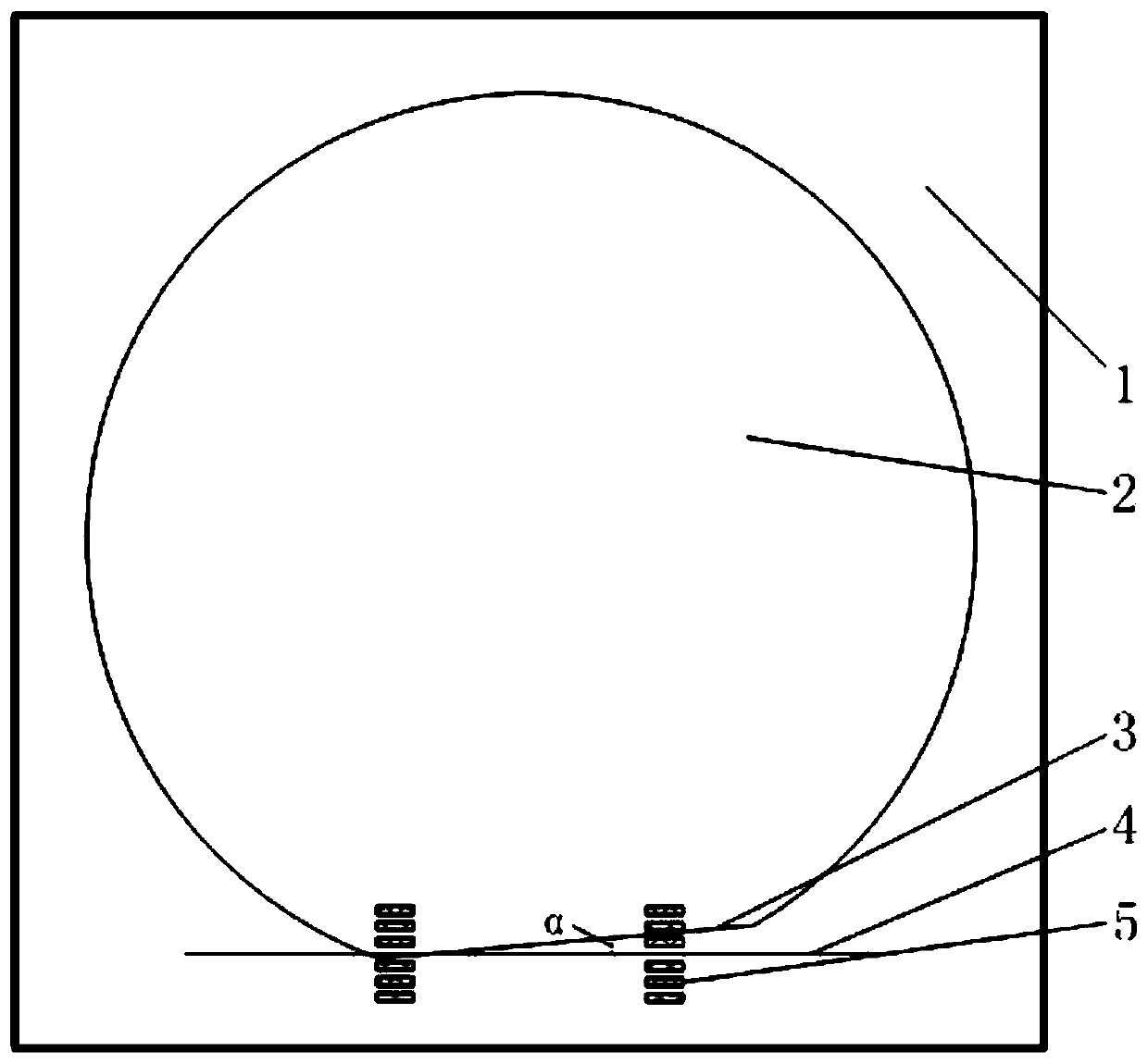
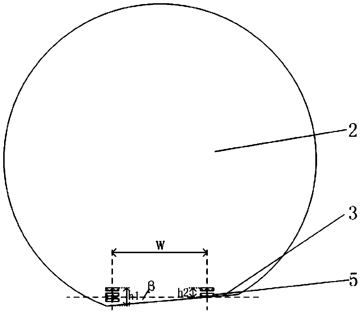
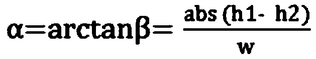
[0010] The invention provides a method for quickly identifying the included angle of a single crystal silicon chip pattern. figure 1 It is a schematic diagram of the alignment of the method for quickly identifying the included angle of a single crystal silicon wafer pattern according to the present invention. In the method, when designing the photoresist plate, two equidistant one-dimensional array identification scales 5 with a certain distance are set in the vertical direction of the alignment line 4 of the photoresist plate 1 . Then in the photolithography process, align the main reference edge of the silicon wafer with the alignment line 4 on the photoresist plate 1, and use the photolithography process to transpose the identificat...


PUM


Abstract

The invention discloses a method for quickly identifying the pattern included angle of a monocrystalline silicon wafer. The method comprises the following steps: arranging two equal-step-pitch one-dimensional array type identification scales (5) at a certain distance in the vertical direction of an alignment line (4) of a photolithography mask (1); transferring the scales (5) on the photolithography mask (1) to the two ends of a main reference side (3) of a silicon wafer (2); observing and reading scale distances (h1, h2) formed by the identification scales (5) and the main reference side (3)of the silicon wafer (2); and performing calculation to obtain the pattern included angle of the monocrystalline silicon wafer. According to the method, the identification scales are arranged on the photolithography mask, the identification scales are transferred to the silicon wafer by adopting a photolithography technique, and quantitative identification of the included angle can be directly carried out under a microscope. The method is simple, effective, high in identification precision and suitable for batch tape-out manufacturing.

Description

technical field [0001] The invention belongs to the technical field of micro-electromechanical technology, and in particular relates to a method for quickly identifying the included angle of a single-crystal silicon wafer pattern. Background technique [0002] The image transposition in the processing flow of the device in the microelectromechanical system (MEMS) is realized by the photolithography process. Photolithography refers to the selective optical radiation and exposure of the photoresist on the medium by using the photoresist plate with a designed pattern, so that the photoresist is patterned and crosslinked, and then the uncrosslinked photoresist is removed by development. That is, the transposition of the design pattern to the pattern on the single crystal silicon wafer is completed. In this process, the alignment of the pattern and the monocrystalline silicon wafer is very important, which directly affects the control of critical dimensions, especially the first...

Claims


Application Information

Patent Timeline
IPC IPC(8): H01L21/68H01L21/66
CPCH01L21/681H01L22/12
Inventor 赵坤帅熊恒余才佳
Owner XIAN FLIGHT SELF CONTROL INST OF AVIC
Why Eureka
Eureka Blog
Learn More