Eureka AIR delivers breakthrough ideas for toughest innovation challenges, trusted by R&D personnel around the world.

Lead-free solder foil for diffusion soldering and method for producing same

A diffusion welding, thin film technology, applied in welding media, manufacturing tools, welding equipment, etc., to achieve the effect of short applicability

Active Publication Date: 2020-03-17
PFARR STANZTECHN
View PDF17 Cites 0 Cited by
  • Summary
  • Abstract
  • Description
  • Claims
  • Application Information

AI Technical Summary

Problems solved by technology

However, said solvents have the disadvantage with regard to work safety and health protection that, according to the description in WO 96 / 19314, they generate organic acids, which must be removed in an additional work sequence in the subsequent course of the welding process. The organic acid

Method used


Image

  • Lead-free solder foil for diffusion soldering and method for producing same
  • Lead-free solder foil for diffusion soldering and method for producing same
  • Lead-free solder foil for diffusion soldering and method for producing same

Examples


Embodiment Construction

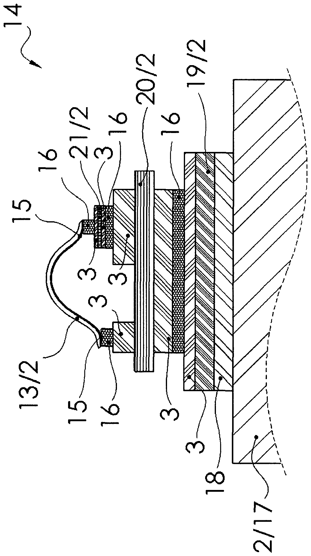
[0078] Subsequently, the solution according to the invention should now be explained in more detail with reference to an exemplary embodiment in conjunction with 5 figures.

[0079] figure 1 A schematic structure of a semiconductor power switch is shown.

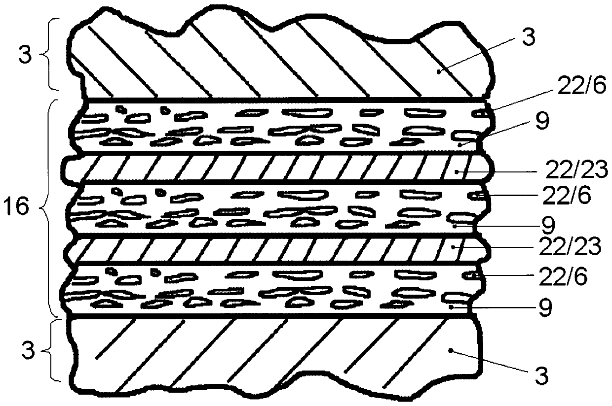
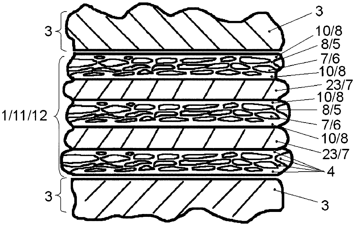
[0080] The chip / semiconductor module 21 is soldered to the conductor track, that is to say the metallic surface layer 3 , which is carried by the electrically insulating layer (DCB) of ceramic construction, ie the ceramic base layer 20 . The upper side of the ceramic base layer is connected to a further conductor track / metallic surface layer 3 , which is likewise located on the base layer, which is generally achieved in a bonding process by means of thin aluminum or copper wires / conductor strips 13 . The base layer 20 of ceramic is welded to the bottom plate 19 which is fitted on the heat sink / cooler 17 . All surfaces / surface layers 3 to be connected must be metallic, and the connection region 16 itself must ensure as effi...


PUM

PropertyMeasurementUnit
Thicknessaaaaaaaaaa
Total thicknessaaaaaaaaaa
Layer thicknessaaaaaaaaaa

Abstract

The invention relates to a lead-free solder foil for diffusion soldering and to the method for producing the same, with which metallic components and / or metallized / metal-coated components, i.e. metallic surface layers of adjacent components, can be connected to one another. The object of the invention is to provide a cost-effective, environmentally friendly and non-toxic, lead-free solder foil fordiffusion soldering with which surface layers of the components to be soldered can be connected to another in such a way that a continuous layer of a high-melting connecting zone in the form of an intermetallic phase with a re-melting temperature of higher than 400 DEG C is produced in a process temperature range typical for soft soldering, i.e. at about 240 DEG C, and in soldering times of lessthan 5 minutes, without a subsequent heat treatment and without a pressing force being exerted during the soldering. The lead-free solder foil (1) according to the invention for diffusion soldering comprises a composite solder material (4), which is produced by roll-bonding and is then roughened in such a way that, in a lead-free soft solder environment of a soft solder matrix (5), compact particles (6) of a high-melting metal component (7) are completely surrounded by the lead-free soft solder (8), wherein the dispersed particles (6) of the high-melting metal component (7) have in the direction of the foil thickness a thickness of 3 microns to 20 microns, the distances between the particles (6) in the soft solder matrix (5) are 1 micron to 10 microns, each of the particles of the high-melting metal component (7) is enclosed on all sides by the 1 micron to 10 microns thick layer of the lead-free soft solder (8), and the solder foil (1) has adjacent to the metallic surface layers (3) ofthe components (2) to be joined an outer encasing layer (10), the layer thickness of which is 2 microns to 10 microns and which consists of soft solder (8).

Description

technical field [0001] The invention relates to a lead-free soldering film for diffusion soldering and a method for its production, by means of which soldering film metallic structural parts and / or metallized / metal-coated structural parts, i.e. It is said that the metallic surface layers of adjacent structural components can be connected to one another. Background technique [0002] Today in electronics and here especially in power electronics, the reliability of the soldering position requires very good mechanical, electrical and thermal properties of the soldering material and of the connection area produced by it, wherein its stability It should now be extended to higher and higher temperature ranges. [0003] Here, for reasons of environmental protection and health concerns, the international trend tends to use lead-free solder materials which are environmentally friendly and health concerns. [0004] In the course of the transition to lead-free solders, numerous, most...

Claims


Application Information

Patent Timeline
IPC IPC(8): B23K35/26B23K35/30B23K35/02
CPCB23K35/262B23K35/302B23K35/0238B23K35/0244H01L2224/48091H01L2224/48227H01L2224/48472H01L2924/00014B23K35/02B23K35/40B23K35/025H01L24/29H01L2924/01327H05K3/3463
Inventor H.达乌德A.洛伊多尔特S.赖歇尔特
Owner PFARR STANZTECHN
Why Eureka
Eureka Blog
Learn More