Shallow trench isolation structure and preparation method thereof
A technology of isolation structures and shallow trenches, which is applied in semiconductor/solid-state device manufacturing, electrical components, circuits, etc., can solve problems such as side trenches, reduce parasitic currents, avoid formation of side trenches, and improve production yield Effect
- Summary
- Abstract
- Description
- Claims
- Application Information
AI Technical Summary
Problems solved by technology
Method used
Image

Examples
Embodiment 1
[0069] Such as Figure 2 to Figure 17 As shown, the present invention provides a method for preparing a shallow trench isolation structure, the method comprising the following steps:
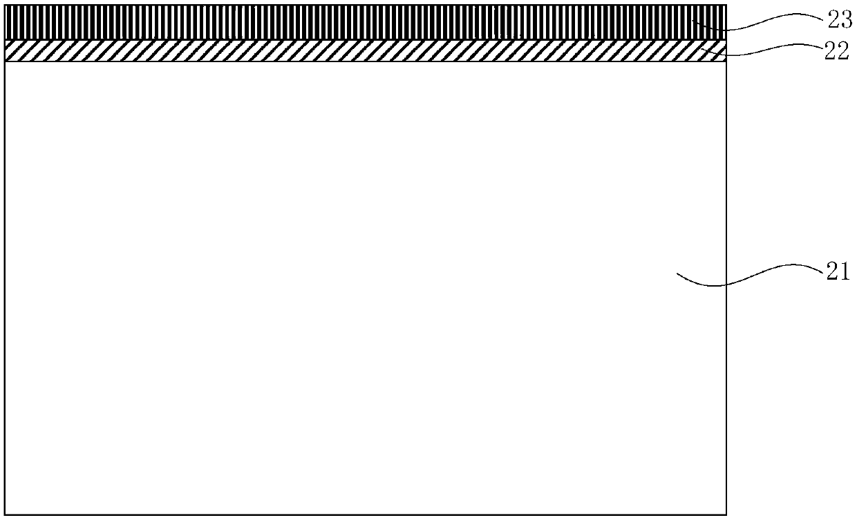
[0070] 1) providing a substrate, and sequentially forming a stacked pad oxide layer and an etching stopper layer on the substrate;
[0071] 2) forming a first opening in the etch stop layer and the pad oxide layer, and forming a first trench in the substrate according to the first opening;
[0072] 3) forming a sidewall protection layer in the first opening and the first trench, the upper surface of the sidewall protection layer being flush with the upper surface of the etching stopper layer;
[0073] 4) forming a hard mask layer on the surface of the etching stopper layer and the sidewall protection layer, and forming a second opening in the hard mask layer;
[0074] 5) forming a second groove in the sidewall protection layer according to the second opening, the lateral dimension of the secon...
Embodiment 2
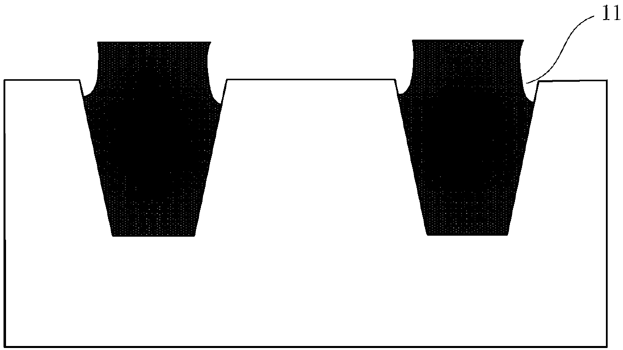
[0099] Such as Figure 17 As shown, the present invention also provides a shallow trench isolation structure, which is obtained by the preparation method described in the first embodiment. Specifically, the shallow trench isolation structure of this embodiment includes:
[0100] Substrate 21;
[0101] The first groove 24 is located in the substrate 21;
[0102] a sidewall protection layer 25, located on the sidewall of the first trench 24, and extending from the bottom of the first trench 24 to above the substrate 21;
[0103] The second groove 27 is partly located in the substrate 21 and inside the sidewall protection layer 25 , the upper surface of the second groove 27 is flat with the upper surface of the sidewall protection layer 25 together;
[0104] The third trench 28 is located in the substrate 21 and at the bottom of the second trench 27, and communicates with the second trench 27;
[0105] a substrate oxide layer 29 located on the sidewall and bottom of the thir...
PUM
| Property | Measurement | Unit |
|---|---|---|
| Thickness | aaaaa | aaaaa |
| Thickness | aaaaa | aaaaa |
| Thickness | aaaaa | aaaaa |
Abstract
Description
Claims
Application Information
PatSnap Eureka turns technology decisions into work you can execute. Powered by our Innovation Knowledge Graph, it runs expert workflows across engineering, life sciences, materials and intellectual property. Get your review-ready output in minutes.


