A kind of electromagnetic wave protective coating and preparation method thereof
A protective coating, electromagnetic wave technology, applied in the coating, metal material coating process, vacuum evaporation coating and other directions, can solve the problem of unsuitable wave absorbing materials, etc., achieves simple preparation method, low synthesis temperature, and low material cost Effect
- Summary
- Abstract
- Description
- Claims
- Application Information
AI Technical Summary
Problems solved by technology
Method used
Image

Examples
Embodiment 1
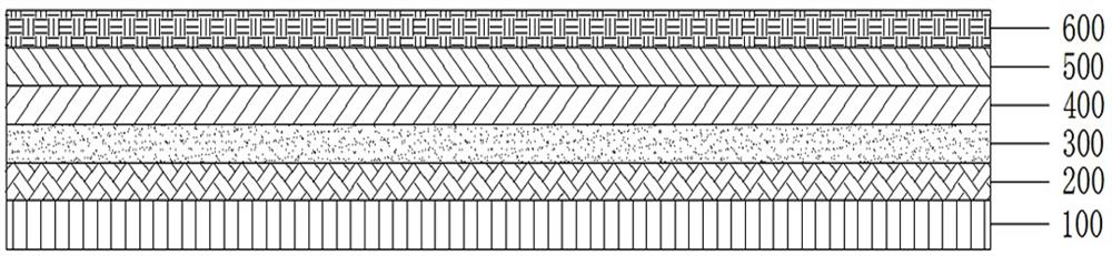
[0025] Embodiment one: if figure 1 As shown, an electromagnetic wave protective coating includes a composite film layer located on the surface of a substrate 100. The composite film layer includes an adhesive layer 200, an inner layer 300, a first transition layer 400, and a second transition layer arranged sequentially from the inside to the outside. Layer 500 and outer layer 600, the bonding layer is an aluminum nickel layer, the inner layer is an aluminum nickel / aluminum oxide layer, the first transition layer is an aluminum oxide / silicon carbide layer, and the second transition layer is a silicon carbide layer / Diamond-like layer, the outer layer is a diamond-like layer, wherein the substrate is used as an outer shell of an electronic device.
[0026] In this embodiment, the contents of aluminum and nickel in the bonding layer are 50%, the contents of aluminum, nickel and aluminum oxide in the inner layer are 35%, 35% and 30% respectively, and the oxide in the first transi...
Embodiment 2
[0037] Embodiment two: if figure 1 As shown, an electromagnetic wave protective coating includes a composite film layer located on the surface of a substrate 100. The composite film layer includes an adhesive layer 200, an inner layer 300, a first transition layer 400, and a second transition layer arranged sequentially from the inside to the outside. Layer 500 and outer layer 600, the bonding layer is an aluminum nickel layer, the inner layer is an aluminum nickel / aluminum oxide layer, the first transition layer is an aluminum oxide / silicon carbide layer, and the second transition layer is a silicon carbide layer / Diamond-like layer, the outer layer is a diamond-like layer, wherein the substrate is used as an outer shell of an electronic device.
[0038] In this embodiment, the contents of aluminum and nickel in the bonding layer are 50%, the contents of aluminum, nickel and aluminum oxide in the inner layer are 35%, 35% and 30% respectively, and the oxide in the first transi...
Embodiment 3
[0049] Embodiment three: as figure 1 as shown in figure 1 As shown, an electromagnetic wave protective coating includes a composite film layer located on the surface of a substrate 100. The composite film layer includes an adhesive layer 200, an inner layer 300, a first transition layer 400, and a second transition layer arranged sequentially from the inside to the outside. Layer 500 and outer layer 600, the bonding layer is an aluminum nickel layer, the inner layer is an aluminum nickel / aluminum oxide layer, the first transition layer is an aluminum oxide / silicon carbide layer, and the second transition layer is a silicon carbide layer / Diamond-like layer, the outer layer is a diamond-like layer, wherein the substrate is used as an outer shell of an electronic device.
[0050] In this embodiment, the contents of aluminum and nickel in the bonding layer are 50%, the contents of aluminum, nickel and aluminum oxide in the inner layer are 35%, 35% and 30% respectively, and the o...
PUM
| Property | Measurement | Unit |
|---|---|---|
| thickness | aaaaa | aaaaa |
| thickness | aaaaa | aaaaa |
| thickness | aaaaa | aaaaa |
Abstract
Description
Claims
Application Information