Semiconductor structure, preparation method and application thereof
A semiconductor and metal structure technology, applied in the fields of semiconductor/solid-state device manufacturing, semiconductor devices, semiconductor/solid-state device components, etc., can solve the problems of poor electrical stability and reliability of semiconductor devices, high contact resistance, etc.
- Summary
- Abstract
- Description
- Claims
- Application Information
AI Technical Summary
Problems solved by technology
Method used
Image

Examples
preparation example Construction
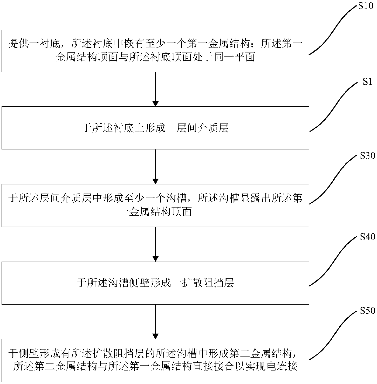
[0119] figure 1 It is a flowchart of the semiconductor structure preparation method of the present invention, and the preparation method includes the following steps:
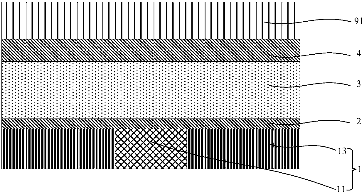
[0120] Execute step S10, such as Figure 2a As shown, a substrate 1 is provided, and at least one first metal structure 11 is embedded in the substrate 1; the top surface of the first metal structure 11 is in the same plane as the top surface of the substrate 1. For example, the substrate 1 may be a general semiconductor structure after completing the front-end process (Front End Of Line, FEOL), and the first metal structure 11 includes electrical connection terminals (for example, transistors) for electrical connection with the outside. gate terminal of a device) or a contact formed on an electrical connection terminal (for example, a contact formed on a source / drain terminal of a transistor device).
[0121] In one embodiment, as image 3 As shown, the substrate 1 also includes a third stop layer 12 and an...
Embodiment approach
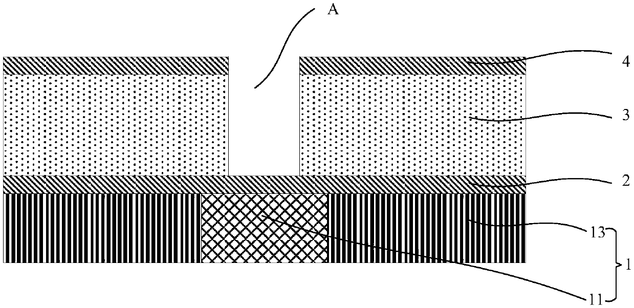
[0138] In the first embodiment, it is necessary to etch and open the first stop layer 2 first. During the process of etching the first stop layer 2, this may cause damage and deformation of the interlayer dielectric layer 3 exposed by the trench, affecting Subsequent filling of the second metal structure further affects the electrical stability and reliability of the finally formed device.
[0139] For this reason, the present invention discloses another kind of embodiment, comprises the following steps: first, as Figure 2b As shown in / 2g, the first groove A / groove B is used as a groove for forming a diffusion barrier layer 5, and a diffusion barrier material 50 is formed on the inner wall of the groove A / groove B; secondly, remove the material 50 located in the groove The diffusion barrier layer material 50 at the bottom of A / trench B, so as to form the diffusion barrier layer 5 on the sidewall of the trench A / trench B, and expose the first stop layer 2; finally , removing...
Embodiment 1
[0162] Such as Figure 2a-2b , as shown in 4a-4d, this embodiment provides a method for preparing a semiconductor structure, which specifically includes the following steps.
[0163] First, if Figure 2a As shown, a substrate 1 is provided, the substrate 1 includes a bottom dielectric layer 13 and a first metal structure 11, the first metal structure 11 is embedded in the bottom dielectric layer 13, and the first metal The top surface of the structure 11 is in the same plane as the top surface of the bottom dielectric layer 13; a first stop layer 2, an interlayer dielectric layer 3, and a second stop layer are sequentially formed on the substrate 1 from bottom to top 4. A third photoresist layer 91; as an example, the thickness of the first stop layer 2 is between 40-70nm, the thickness of the interlayer dielectric layer 3 is between 250nm-300nm, and the second stop layer The thickness of the layer 4 is 200%~250% of the thickness of the first stop layer 2, which is to preven...
PUM
| Property | Measurement | Unit |
|---|---|---|
| thickness | aaaaa | aaaaa |
| thickness | aaaaa | aaaaa |
| thickness | aaaaa | aaaaa |
Abstract
Description
Claims
Application Information
 - R&D
- Intellectual Property
- Life Sciences
- Materials
- Tech Scout
- Unparalleled Data Quality
- Higher Quality Content
- 60% Fewer Hallucinations
Browse by: Latest US Patents, China's latest patents, Technical Efficacy Thesaurus, Application Domain, Technology Topic, Popular Technical Reports.
© 2025 PatSnap. All rights reserved.Legal|Privacy policy|Modern Slavery Act Transparency Statement|Sitemap|About US| Contact US: help@patsnap.com