Multi-patterning method and memory forming method
A multi-patterning and memory technology, used in semiconductor/solid-state device manufacturing, electrical components, circuits, etc., can solve the problems of lithography process accuracy limitations, inability to flexibly adjust the pattern size, etc., and achieve the effect of small-sized pattern preparation
- Summary
- Abstract
- Description
- Claims
- Application Information
AI Technical Summary
Problems solved by technology
Method used
Image
Examples
Embodiment 1
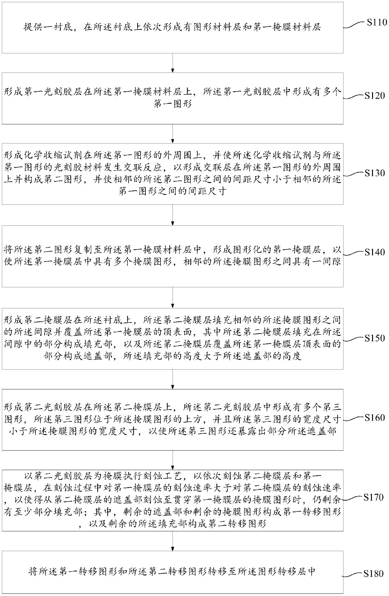
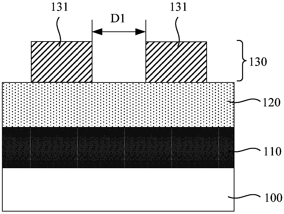
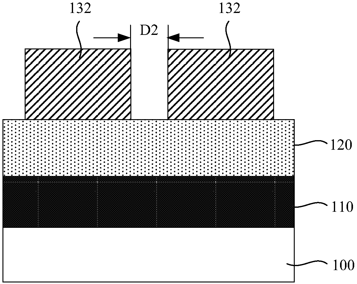
[0073] figure 1 It is a schematic flow chart of the multiple graphics method in Embodiment 1 of the present invention, Figure 2a ~ Figure 2f It is a schematic structural diagram of the multi-patterning method in the first embodiment of the present invention during its patterning process, and each step in the first embodiment of the present invention will be described in detail below with reference to the accompanying drawings.
[0074] In step S110, specifically refer to Figure 2a As shown, a substrate 100 is provided, on which a pattern transfer layer 110 and a first mask material layer 120 are sequentially formed. In the subsequent process, the pattern to be transferred is defined on the pattern transfer layer 110 , and the defined pattern is further transferred into the pattern transfer layer 110 .
[0075] In step S120, continue to refer to Figure 2a As shown, a first photoresist layer 130 is formed on the first mask material layer 120 , and a plurality of first patt...
Embodiment 2
[0093] image 3 It is a schematic flow chart of the forming method of the memory in Embodiment 2 of the present invention, Figure 4a ~ Figure 4g It is a structural schematic diagram of the memory in the second embodiment of the present invention during its formation process. Each step in this embodiment will be described in detail below with reference to the accompanying drawings.
[0094] In step S210, specifically refer to Figure 4a As shown, a substrate 200 is provided, and a plurality of active regions AA are defined on the substrate 200, node contact areas NCA are respectively provided on opposite ends of the active regions AA, and on the substrate A dielectric layer 270 and a first mask material layer 220 are also sequentially formed on the bottom 100 .
[0095] In the subsequent process, the first mask material layer 220 is used to define a desired pattern on the dielectric layer 270 , and the defined pattern is transferred to the dielectric layer 270 . Further, t...
Embodiment 3
[0126] The difference from Embodiment 2 is that in this embodiment, after forming the dielectric layer and before forming the first mask material layer, it further includes: performing a planarization process on the dielectric layer to reduce the dielectric layer layer height.
[0127] Figure 5a It is a structural schematic diagram of the method for forming the memory in Embodiment 3 of the present invention after the dielectric layer is planarized. like Figure 5a As shown, in this embodiment, the dielectric layer 270 is planarized, and planarized to the cover layer of the bit line BL (that is, after the planarization process, the position of the top surface of the dielectric layer 270 is, for example, between the top surface location and the bottom surface location of the capping layer of the bit line BL). At this time, on the basis of reducing the height of the dielectric layer 270 , it is also possible to prevent the conductive layer in the bit line BL from being expos...
PUM
 Abstract
Description
Claims
Application Information


