Preparation method and application of sub-10 nanometer gap structure
A technology of nano-gap and electron beam, applied in the field of nano-processing
- Summary
- Abstract
- Description
- Claims
- Application Information
AI Technical Summary
Problems solved by technology
Method used
Image
Examples
Embodiment 1
[0054] A sub-10 nanometer gap structure, the preparation method is as follows:
[0055] (1) Use GDSII software to design such as figure 1 The overlapping pattern of the top structure is shown, wherein the angle of the top is 5°, and the overlapping length is 200nm.
[0056] (2) Soak the silicon wafer in acetone, isopropanol and deionized water and ultrasonically clean it, blow it dry with nitrogen, then spin-coat a layer of PMMA glue with a thickness of 80nm, and bake it in an oven at a temperature of 180°C for a period of 5 minutes.
[0057] (3) Electron beam exposure is carried out on the substrate, the electron beam acceleration voltage used is 100kV, the beam current is 100pA, the exposure step length is 1nm, and the exposure dose is 700μC / cm 2 .
[0058] (4) Develop in a mixture of methyl isobutyl pentanone and isopropanol (1:3) for 30 s, fix in isopropanol for 30 s, and blow dry gently with nitrogen to obtain a sub-10 nanometer gap structure mask .
Embodiment 2
[0060] A sub-10 nanometer gap structure, the preparation method is as follows:
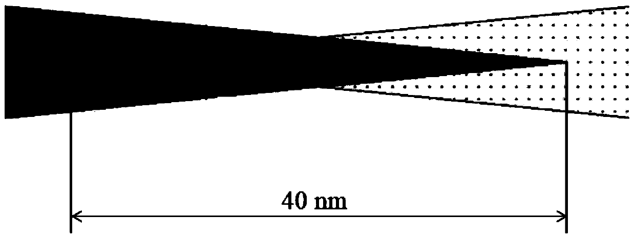
[0061] (1) Use GDSII software to design such as figure 2 The overlapping pattern of the top structure is shown, wherein the apex angle is 10°, and the overlapping length is 40nm.
[0062] (2) Soak the silicon wafer in acetone, isopropanol and deionized water and ultrasonically clean it, blow it dry with nitrogen, then spin-coat a layer of PMMA glue with a thickness of 80nm, and bake it in an oven at a temperature of 180°C for a period of 5 minutes.
[0063] (3) Electron beam exposure is carried out on the substrate, the electron beam acceleration voltage used is 100kV, the beam current is 100pA, the exposure step length is 1nm, and the exposure dose is 700μC / cm 2 ;
[0064] (4) Develop in a mixture of methyl isobutyl pentanone and isopropanol (1:3) for 30 s, fix in isopropanol for 30 s, and blow dry gently with nitrogen to obtain a sub-10 nanometer gap structure mask .
Embodiment 3
[0066] A sub-10 nanometer gap structure, the preparation method is as follows:
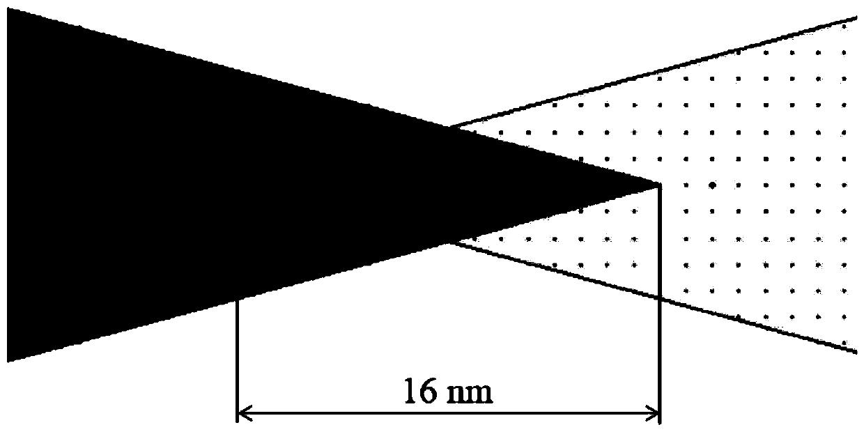
[0067] (1) Use GDSII software to design such as image 3 The overlapping pattern of the top-to-top structure is shown, wherein the apex angle is 30°, and the overlapping length is 16nm.
[0068] (2) Soak the silicon wafer in acetone, isopropanol and deionized water and ultrasonically clean it, blow it dry with nitrogen, then spin-coat a layer of PMMA glue with a thickness of 80nm, and bake it in an oven at a temperature of 180°C for a period of 5 minutes.
[0069] (3) Electron beam exposure is carried out on the substrate, the electron beam acceleration voltage used is 100kV, the beam current is 100pA, the exposure step length is 1nm, and the exposure dose is 700μC / cm 2 ;
[0070] (4) Develop in a mixture of methyl isobutyl pentanone and isopropanol (1:3) for 30 s, fix in isopropanol for 30 s, and blow dry gently with nitrogen to obtain a sub-10 nanometer gap structure mask .
PUM
| Property | Measurement | Unit |
|---|---|---|
| Top angle | aaaaa | aaaaa |
| Length | aaaaa | aaaaa |
| Thickness | aaaaa | aaaaa |
Abstract
Description
Claims
Application Information


