A method and simulation method for determining the prohibition period of photolithography process nodes

A technology of lithography process and simulation method is applied in the field of determining the prohibition period of lithography process nodes, which can solve the problems of tediousness, inability to effectively guide the formulation of layout design rules, and inaccurate prohibition periods.

Active Publication Date: 2021-08-13
INST OF MICROELECTRONICS CHINESE ACAD OF SCI
View PDF0 Cites 0 Cited by
  • Summary
  • Abstract
  • Description
  • Claims
  • Application Information

AI Technical Summary

Problems solved by technology

[0006] In view of the above analysis, the present invention aims to provide a method and simulation method for determining the prohibition period of the lithography process node, which is not only very cumbersome to solve the existing method of finding out the prohibition period, but also has the inaccuracy of the prohibition period found. , so that it is impossible to effectively guide the formulation of layout design rules, and it is impossible to judge the reasons for the poor quality of individual graphic lithography in the lithography stage

Method used


Image

  • A method and simulation method for determining the prohibition period of photolithography process nodes
  • A method and simulation method for determining the prohibition period of photolithography process nodes
  • A method and simulation method for determining the prohibition period of photolithography process nodes

Examples


Embodiment 1

[0048] A specific embodiment of the present invention discloses a method for finding out the lithography forbidden period (forbiddenpitch, FP) by calculation simulation, such as Figure 14 shown, including the following steps:

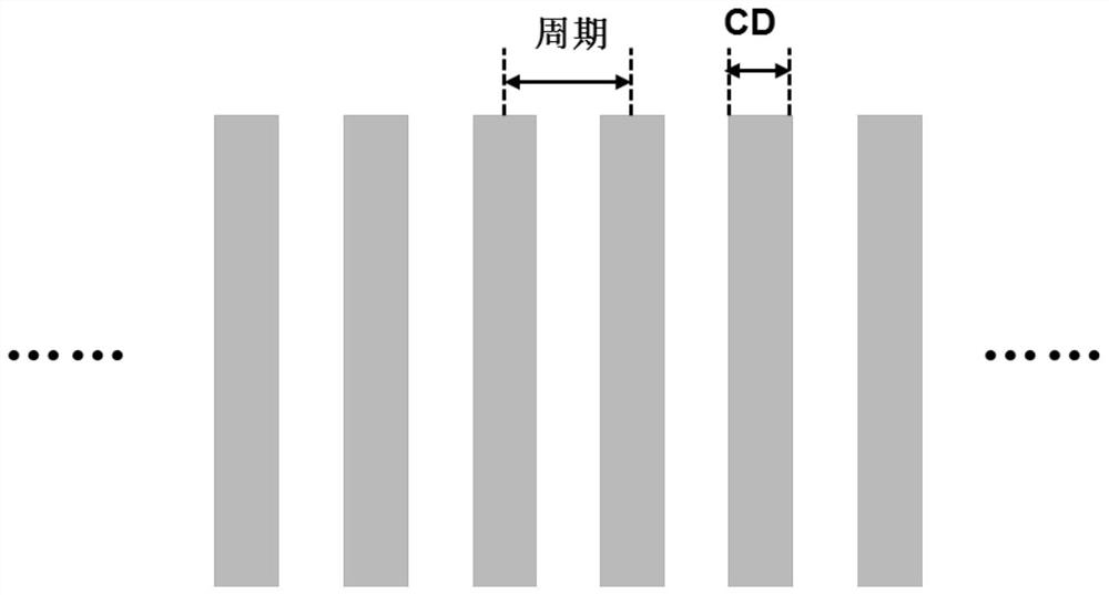
[0049] Step 1: Obtain a test pattern (test pattern), mainly a one-dimensional variable-period line (through pitch) pattern within a certain range, and the line width (critical dimension, CD) is the key line width (ie, key dimension) of the lithography node , for example, the actual key line width of the 14nm node is 38nm, and the period (pitch) should include as much as possible;

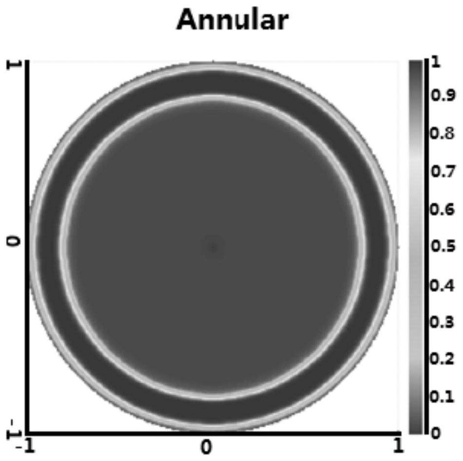
[0050] Step 2: Set initial simulation light source parameters (for example, a circular light source or a ring light source is used as the initial light source, and a ring light source is used as the initial light source in this embodiment) and related simulation parameters, such as the model of the lithography machine, NA (numerical aperture) value, Reticle parameters and p...

Embodiment 2

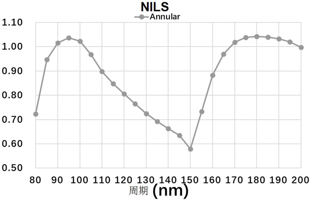
[0060] The resolution limit size of the 193nm immersion lithography technology is 76nm. In this embodiment, we use a test pattern with a minimum period of 80nm. First obtain the test pattern (test pattern), mainly one-dimensional variable period (the present embodiment is 80nm-200nm) line (through pitch) pattern within a certain range, such as Figure 8 shown. The line width (CD) is the minimum dimension of the lithography node. In this embodiment, a one-dimensional pattern with CD=40nm is selected, and the period (pitch) includes as much as possible. Set the parameters of the initial simulated light source (for example, a circular light source or a ring light source is used as the initial light source, and the ring light source selected in this embodiment is used as the initial light source, such as Figure 9 shown. Relevant simulation parameters include lithography machine model NXT1950i, NA (numerical aperture) value of 1.35, mask plate parameters, photoresist parameters,...

Embodiment 3

[0070] A specific embodiment of the present invention discloses a method for improving photolithography performance by optimizing a one-dimensional line pattern structure in which prohibited periods and dense periods are alternately arranged, including the following steps:

[0071] Step 1: Obtain an optimized free light source considering the global situation. Obtain various types of test patterns as comprehensive as possible from the actual layout as the initial layout input. Initial light source parameters (generally, a ring light source is used as the initial light source) and related simulation parameters include lithography machine model, NA (numerical aperture) value, mask plate parameters (thickness, refractive index, etc.), etc.;

[0072] Step 2: Under the above parameter settings, use professional simulation software to perform collaborative optimization of light source mask (SMO) to obtain the optimized free light source (freeform source1), and analyze the data to fi...


PUM


Abstract

The invention relates to a method and a simulation method for determining the prohibition period of a lithography process node, belonging to the technical field of semiconductor lithography, and solves the problem that the prohibition period found in the method is inaccurate, cannot effectively guide the formulation of layout design rules, and in the lithography stage The problem that it is impossible to determine the reason for the poor quality of individual pattern lithography. The method for determining the prohibition period of the lithography process node includes the following steps: obtaining a test pattern; setting the first light source and simulation parameters, and using software to simulate; analyzing the simulation results, making the first curve, and finding out the first curve that is obviously lower than The cycle range of other values ​​(the first cycle range); set the second light source and light source parameters, and make the second curve; find out the cycle range (second cycle range) that is obviously lower than other values ​​in the second curve, and combine the second cycle The range and the first cycle range jointly determine the prohibited cycle range. The invention realizes simple, efficient and accurate determination of the prohibition period under the technical node.

Description

technical field [0001] The invention relates to the technical field of semiconductor photolithography, in particular to a method and a simulation method for determining a prohibition period of a photolithography process node. Background technique [0002] Lithography technology enters the node below 20nm and faces greater challenges. Although many resolution enhancement techniques have been adopted, such as source mask collaborative optimization (SMO), optical proximity correction (OPC), or adding sub-resolution auxiliary graphics (Sbar), etc. However, due to some insurmountable problems, the increase of the process window still faces great challenges, for example, the forbidden period (forbidden pitch, FP) effect. There will be some forbidden periods in lithography, that is, patterns within this size range will cause the process window of the entire layout to become smaller, and the quality of lithography will be significantly deteriorated. [0003] In the design stage of ...

Claims


Application Information

Patent Timeline
Patent Type & Authority Patents(China)
IPC IPC(8): G03F7/20
CPCG03F7/70G03F7/70425G03F7/70625
Inventor 何建芳韦亚一粟雅娟董立松张利斌苏晓菁陈睿马玲
Owner INST OF MICROELECTRONICS CHINESE ACAD OF SCI
Why Eureka
Try Eureka