Automatic wafer loading and unloading system

A wafer and automatic technology, applied in electrical components, semiconductor/solid-state device manufacturing, circuits, etc., can solve the problems of high worker mobility and labor difficulties, avoid wafer pollution, solve labor difficulties, and huge economic benefits. Effect

Active Publication Date: 2020-04-17
SHANGHAI FORESIGHT ROBOTICS CO LTD
View PDF6 Cites 0 Cited by
  • Summary
  • Abstract
  • Description
  • Claims
  • Application Information

AI Technical Summary

Problems solved by technology

[0006] The purpose of the present invention is to overcome the above-mentioned defects in the prior art, and provide an automatic wafer loading and unloading system to improve the efficiency of the entire produ

Method used


Image

  • Automatic wafer loading and unloading system
  • Automatic wafer loading and unloading system
  • Automatic wafer loading and unloading system

Examples


Example Embodiment

[0028] The specific embodiments of the present invention will be further described in detail below with reference to the accompanying drawings.

[0029] It should be noted that in the following specific embodiments, when the embodiments of the present invention are described in detail, in order to clearly show the structure of the present invention for ease of description, the structure in the drawings is not drawn according to the general scale. Partial enlargement, deformation, and simplification of processing have been implemented. Therefore, this should be avoided as a limitation of the present invention.

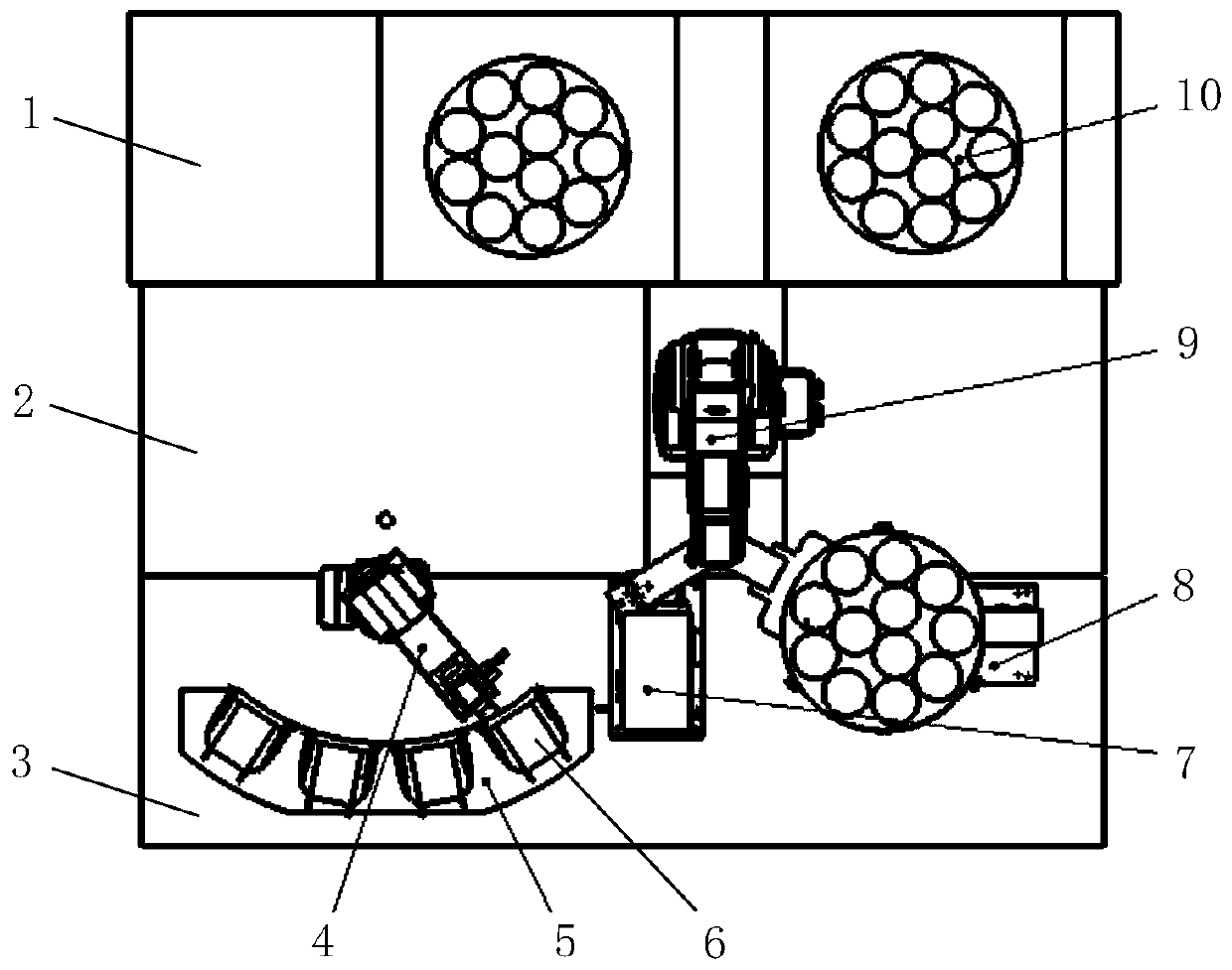
[0030] In the following specific embodiments of the present invention, please refer to figure 1 , figure 1 It is a schematic structural diagram of a wafer automatic loading and unloading system according to a preferred embodiment of the present invention. Such as figure 1 As shown, an automatic wafer loading and unloading system of the present invention, integrated with proc...


PUM


Abstract

The invention discloses an automatic wafer loading and unloading system. The system comprises a storage unit integrated on process equipment, a wafer positioning unit, a wafer disc positioning unit and a wafer disc storage unit. A first loading unit is adopted to transmit wafer discs before and after the process between the wafer disc storage unit and the wafer disc positioning unit, and a secondloading unit is adopted to transmit wafers before and after the process among the wafer disc positioning unit, the wafer positioning unit and a storage unit. According to the system, the efficiency ofthe whole production process can be improved, wafer pollution is avoided, the percent of pass of the wafers placed in the wafer disc is improved, and the rejection rate of the wafers is reduced.

Description

technical field [0001] The invention relates to the technical field of automatic control of semiconductor equipment, in particular to an integrated wafer automatic loading and unloading system. Background technique [0002] In the wafer epitaxial PVD (Physical Vapor Deposition) process, it is necessary to place the wafer before deposition on the silicon carbide wafer disk, and after high-temperature deposition in the process equipment, the wafer is removed from the silicon carbide wafer disk out. [0003] At present, it is generally used to manually move the deposited FOUP (front-opening wafer transfer box) with multiple silicon carbide wafers from the PVD equipment to a position, and manually deposit each silicon carbide wafer The final wafer is taken out, and the other wafers before deposition are placed in the silicon carbide wafer tray. [0004] However, the problem of low pass rate occurs during manual operation. Since the wafer transportation is exposed to the ordin...

Claims


Application Information

Patent Timeline
IPC IPC(8): H01L21/677
CPCH01L21/67739H01L21/67763
Inventor 陈朝星
Owner SHANGHAI FORESIGHT ROBOTICS CO LTD
Why Eureka
Try Eureka