Wafer chamfering process

A round wafer and chamfering technology, which is applied in the direction of manufacturing tools, grinding workpiece supports, metal processing equipment, etc., can solve the problems that the edge does not meet the standard requirements, the friction time of chamfering is long, and it shrinks when it becomes cold, so as to improve the chamfering. Angle effect, reduce the magnitude of thermal expansion and contraction, and reduce the volume of the part

Active Publication Date: 2020-04-21
上海磐盟电子材料有限公司
View PDF9 Cites 2 Cited by
  • Summary
  • Abstract
  • Description
  • Claims
  • Application Information

AI Technical Summary

Problems solved by technology

[0004] When the wafer is chamfered, the angle between its side and the chamfering groove of the chamfering device will not change. When the side of the wafer just contacts the inner wall of the chamfering groove, the force on the side of the wafer is the largest , due to the symmetry of the two sides of the side, the side of the wafer is not easy to be chamfered, and the friction time of the chamfer is long. After the internal temperature rises, the internal structure of the wafer will expand when heated, and it will shrink after chamfering, thus Make the chamfered edge not meet the standard requirements

Method used


Image

  • Wafer chamfering process
  • Wafer chamfering process

Examples


Embodiment 1

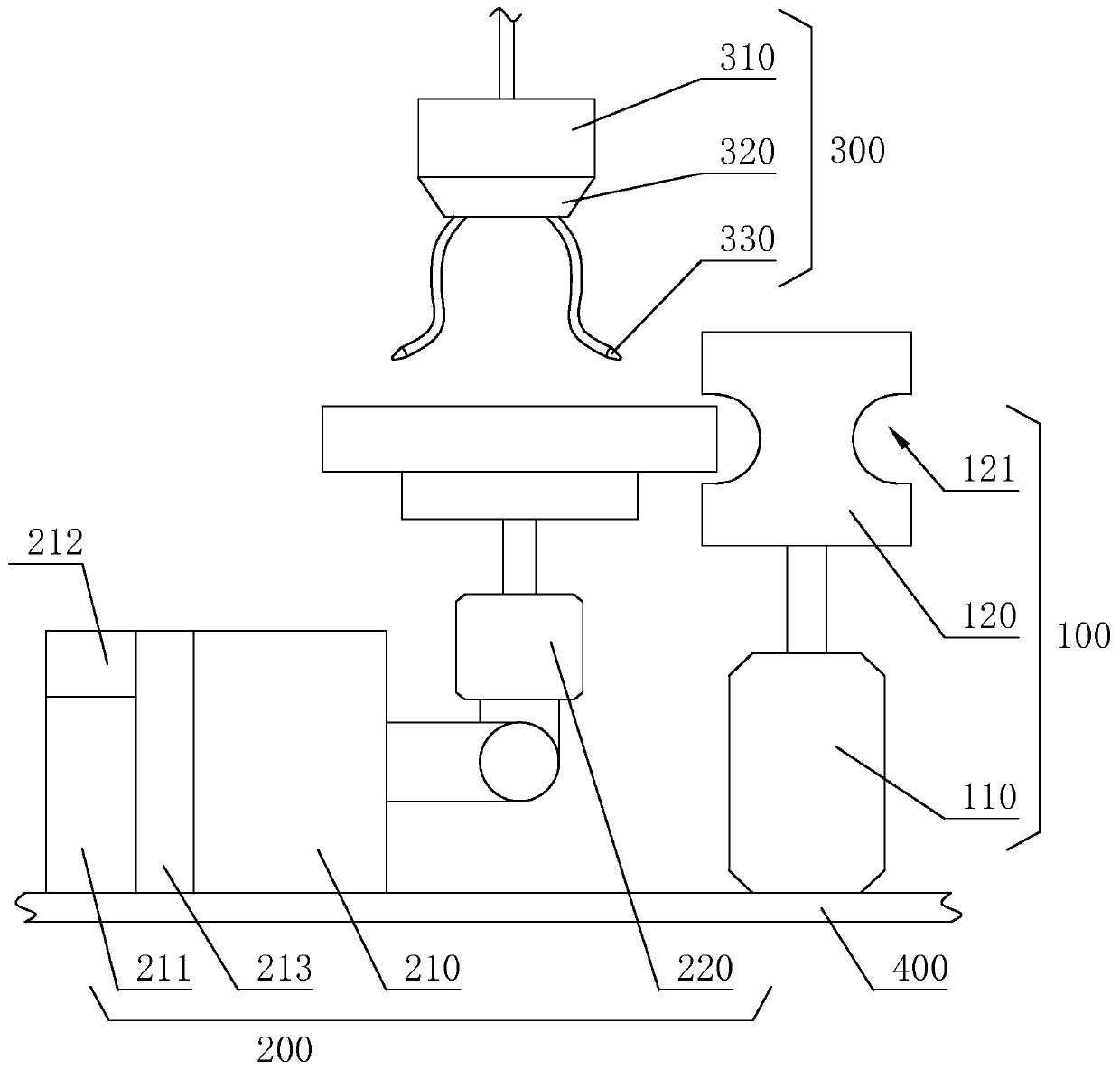
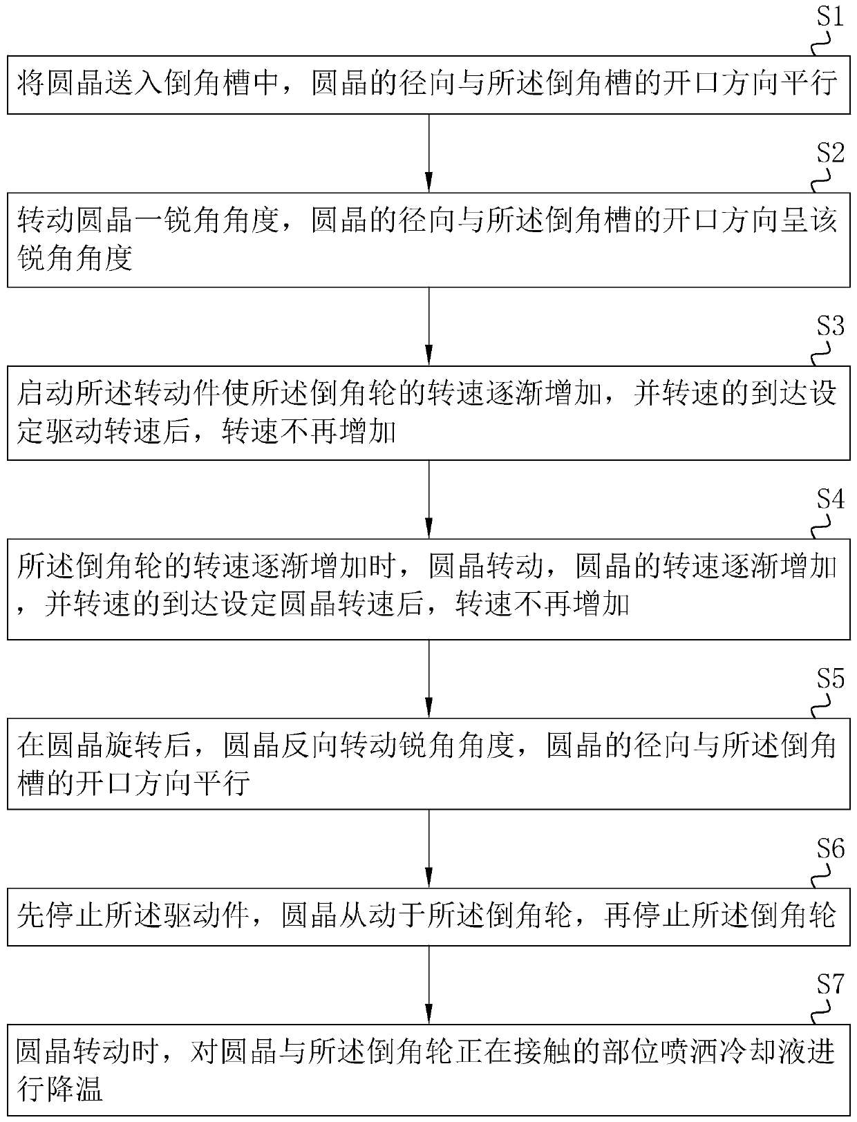
[0034] A wafer chamfering process, such as figure 1 As shown, based on the wafer chamfering device 100 for chamfering the wafer, the fixing jig 200 for installing the wafer, and the cooling assembly 300 for cooling the wafer chamfering device 100 and the wafer, the wafer chamfering The device 100 , the fixing fixture 200 and the cooling assembly 300 are fixed on the workbench 400 through bolt connection or welding, and the cooling assembly 300 is fixed on the workbench 400 through suspender welding.

[0035] The wafer chamfering device 100 includes a rotating part 110 fixed on the upper end of the workbench 400 by bolting or welding. The rotating part 110 can be a motor connected to the mains. A chamfering wheel 120 is connected, the axis line of the chamfering wheel 120 is vertically arranged, and the chamfering wheel 120 can be a grinding wheel. The side of the chamfering wheel 120 is provided with an arc-shaped chamfering groove 121, and the opening direction of the chamfe...

Embodiment 2

[0048] A wafer chamfering process, the difference from Embodiment 1 is that the rotation direction of the wafer is the same as the rotation direction of the chamfering wheel 120, and the rotation speed of the wafer is lower than the rotation speed of the chamfering wheel 120. When chamfering, the wafer The direction of rotation of the parts where the chamfering wheels 120 contact each other is opposite, so that the speed of the wafer chamfering process can be increased.


PUM


Abstract

The invention relates to the technical field of wafer machining, and discloses a wafer chamfering process based on a wafer chamfering device. The wafer chamfering device comprises a rotating piece, the rotating piece is connected with a chamfering wheel, the chamfering wheel is provided with a chamfering groove, and the opening direction of the chamfering groove is perpendicular to the axial direction of the chamfering wheel; the process comprises the following steps that S1, wafers are fed into the chamfering groove; S2: the radial direction of the wafers is at an acute angle with the openingdirection of the chamfered groove; S3, the rotating piece is started to gradually increase the rotating speed of the chamfering wheel, and after the rotating speed reaches a set driving rotating speed, the rotating speed is no longer increased; S4, when the rotating speed of the chamfering wheel is gradually increased, the rotating speed of the wafers is gradually increased, and after the rotating speed reaches the set wafer rotating speed, the rotating speed is no longer increased; and S5, the wafers rotate the acute angle in a reverse mode, and the radial direction of the wafers is parallelto the opening direction of the chamfering groove; and when the chamfering is conducted, the contact area between the wafers and the inner wall of the chamfering groove is reduced, the volume of theparts affected by the temperature change of the wafers is reduced, and the chamfering effect of the edge of the wafers is improved.

Description

technical field [0001] The invention relates to the technical field of wafer processing, more specifically, it relates to a wafer chamfering process. Background technique [0002] Wafer refers to the silicon chip used in the manufacture of silicon semiconductor integrated circuits. Because of its circular shape, it is called wafer. Wafer is the carrier used in the production of integrated circuits. In general, wafers refer to single crystal silicon wafers. Single crystal silicon wafers are drawn and refined from ordinary silica sand, and are made into single crystal silicon rods through a series of measures of dissolution, purification and distillation. After the single crystal silicon rods are polished and sliced, they become wafers. [0003] After cutting, the edge surface of the silicon wafer has edges, corners, burrs, chipping, even cracks or other defects, and the edge surface is relatively rough. In order to increase the mechanical strength of the edge surface of the...

Claims


Application Information

Patent Timeline
Patent Type & Authority Applications(China)
IPC IPC(8): B24B1/00B24B9/06B24B41/06B24B41/04B24B55/02B24B41/02
CPCB24B1/00B24B9/065B24B41/02B24B41/04B24B41/06B24B55/02
Inventor 李茂欣陈海军
Owner 上海磐盟电子材料有限公司
Why Eureka
Try Eureka