SiC power device integrated with fast recovery diode

A technology for recovering diodes and power devices, applied in diodes, semiconductor devices, electrical components, etc., can solve the problems of slow turn-off of SiC IGBTs, inability to use conventional silicon-based reverse-conducting structures, and large reverse-recovery charges. Effects of reverse recovery spike current, reduction of reverse recovery charge and associated losses, and improved cathode injection efficiency

Active Publication Date: 2020-04-21
UNIV OF ELECTRONIC SCI & TECH OF CHINA
View PDF3 Cites 7 Cited by
  • Summary
  • Abstract
  • Description
  • Claims
  • Application Information

AI Technical Summary

Problems solved by technology

[0004] The purpose of the present invention is to propose a new type of SiC MOSFET and IGBT for the shortcomings of SiC MOSFET and IGBT antiparallel PN junction b

Method used


Image

  • SiC power device integrated with fast recovery diode
  • SiC power device integrated with fast recovery diode
  • SiC power device integrated with fast recovery diode

Examples


Embodiment 1

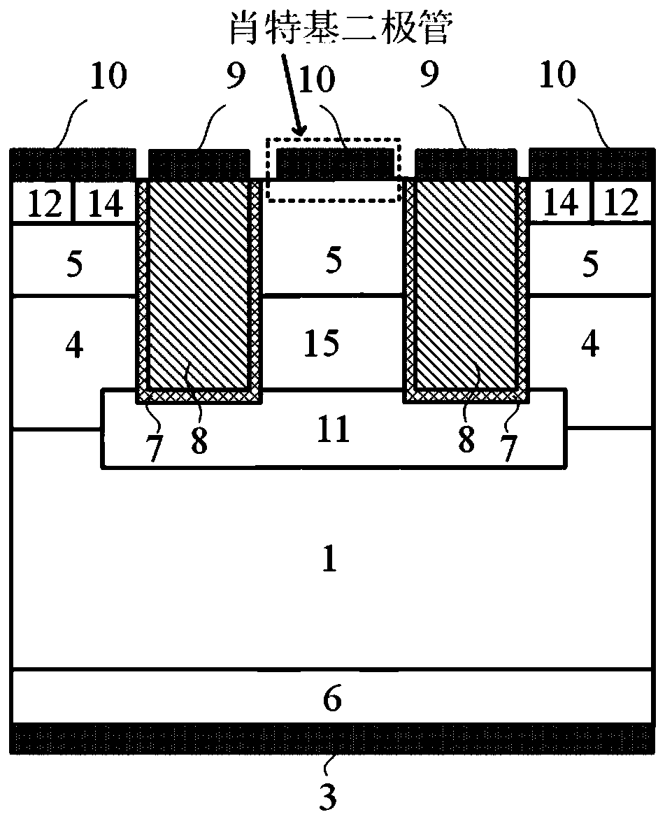
[0039] This embodiment provides a trench gate SiC MOSFET device integrating a PN junction diode, and its cell structure is as follows: figure 1 As shown, it includes: an N-type lightly doped region 1 as a withstand voltage region;

[0040] An N-type heavily doped ohmic contact region 6 is provided on the lower surface of the N-type withstand voltage region 1, and an anode metal 3 covering the lower surface of the N-type heavily doped ohmic contact region 6 is used to form a MOSFET device;

[0041] The upper surface of the N-type withstand voltage region 1 is provided with a P-type semiconductor base region 5 and two gate deep grooves, and the two gate deep grooves divide the P-type semiconductor base region 5 into three independent sub-regions , called the first sub-region, the second sub-region, and the third sub-region from left to right or from right to left; the lower surfaces of the first sub-region and the third sub-region are respectively provided with heavily doped N ...

Embodiment 2

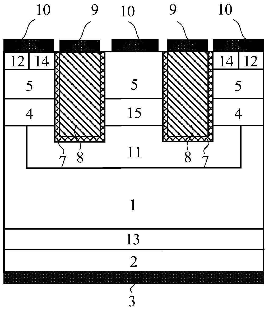
[0045] For this embodiment, a trench-gate SiC IGBT device with a carrier storage layer is provided, and its cell structure is as follows figure 2 Shown; Its difference with embodiment 1 is: the N-type semiconductor buffer layer 13 is arranged on the lower surface of the N-type withstand voltage region 1, and the P-type anode region 2 is arranged on the lower surface of the N-type semiconductor buffer layer 13, so The lower surface of the P-type anode region 2 is covered with an anode metal 3; it is used to form an IGBT device;

[0046] When the IGBT device withstands voltage, the potential of the N-type carrier storage layer 4 is clamped very low by the conduction PMOS and the P-type Schottky diode, so the N-type carrier storage layer 4 can be heavily doped and Will not cause premature breakdown of the device. Due to the heavy doping of the N region 4, a large number of holes injected into the withstand voltage region from the bottom anode P region will be blocked by the bui...

Embodiment 3

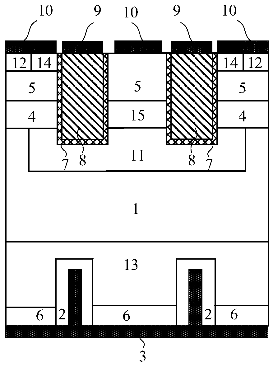
[0048] This embodiment provides a reverse conduction SiC IGBT device, the cell structure of which is as follows image 3 shown; it is different from Embodiment 2 in that: the lower surface of the N-type withstand voltage region 1 is provided with an N-type semiconductor buffer layer 13, and the N-type semiconductor buffer layer 13 is provided with a plurality of The anode deep groove is filled with anode metal 3; the deep groove is surrounded by a P-type anode region 2, and the anode region 2 is not in contact with the N-type withstand voltage region 1; the phase A heavily doped N-type ohmic contact region 6 is arranged between adjacent P-type anode regions 2, and the adjacent P-type anode regions are not in contact, and are isolated by the N-type semiconductor buffer layer (13) in the middle; the P-type anode The region 2, the N-type ohmic contact region 6 is in contact with the anode metal 3 covering the lower surface of the semiconductor; it is used to form a reverse conduc...


PUM


Abstract

The invention relates to the field of power semiconductors, and particularly provides a SiC power device integrated with a fast recovery diode. The SiC power device comprises a SiC MOSFET and a SiC IGBT, wherein for the SiC MOSFET device integrated with a PN junction body diode, the reverse recovery charge and related loss of the body diode can be greatly reduced, the reverse recovery peak currentis reduced, and the EMI noise is reduced; for a reverse conducting SiC IGBT integrated with a PN junction body diode, the reverse recovery charge and related loss of the body diode can be greatly reduced, the reverse recovery peak current is reduced, and the EMI noise is reduced; and meanwhile, by arranging an anode deep groove at the bottom and designing the depth of the anode deep groove and the distance between the grooves, the resistance of an electron flowing path is adjusted, and the output characteristic of the reverse conducting IGBT can enter a bipolar working mode without turning ina unit cell.

Description

technical field [0001] The invention relates to the field of power semiconductors, and specifically provides a SiC power device with low turn-on voltage drop, fast turn-off characteristics and integrated reverse fast recovery diode, including SiC MOSFET and SiC IGBT. Background technique [0002] As a new generation of power semiconductor devices, SiC power semiconductor devices have the characteristics of lower conduction loss, faster switching frequency and better thermal characteristics compared with traditional silicon-based devices; as a mainstream product of power semiconductor devices MOSFETs and IGBTs are favored among SiC materials. In MOSFET or IGBT applications, it is often necessary to connect a fast-recovery high-voltage freewheeling diode in anti-parallel. SiC MOSFET itself integrates a PiN body diode, but due to the large band gap of SiC, the inherent conduction voltage drop of its PN junction is about 3V, so the conduction loss of the body diode is very larg...

Claims


Application Information

Patent Timeline
IPC IPC(8): H01L29/86H01L29/06
CPCH01L29/8613H01L29/0603H01L29/0611H01L29/0684
Inventor 易波赵青谢欣桐张浩悦陈星弼
Owner UNIV OF ELECTRONIC SCI & TECH OF CHINA
Why Eureka
Try Eureka