Light-emitting diode and manufacturing method thereof

A light-emitting diode and light-emitting layer technology, applied in the direction of electrical components, circuits, semiconductor devices, etc., can solve the problems of terminal product modules that cannot operate normally and reduce product stability, and achieve both light extraction efficiency and interlayer stress intensity. Effect of High Light Extraction Efficiency

Active Publication Date: 2020-04-21
XIAMEN SANAN OPTOELECTRONICS CO LTD
View PDF12 Cites 3 Cited by
  • Summary
  • Abstract
  • Description
  • Claims
  • Application Information

AI Technical Summary

Problems solved by technology

[0002] see figure 1 In consideration of the light extraction efficiency, the electrode structure design of the existing LED chip adds a high-reflectivity material to the electrode structure as the reflective layer 200 to improve light efficiency, but most of the high-reflective materials: such as silver, aluminum, etc., have poor characteristics. The stability of the product is reduced by the influence of the environment, temperature, humidity, pH, etc., so a metal protection layer 230 with low m

Method used


Image

  • Light-emitting diode and manufacturing method thereof
  • Light-emitting diode and manufacturing method thereof
  • Light-emitting diode and manufacturing method thereof

Examples


Example Embodiment

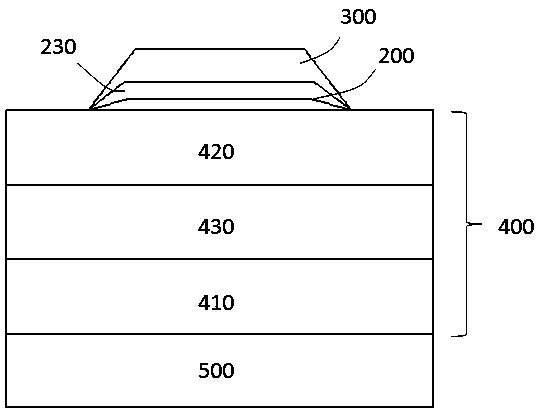
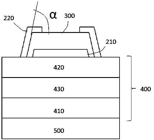
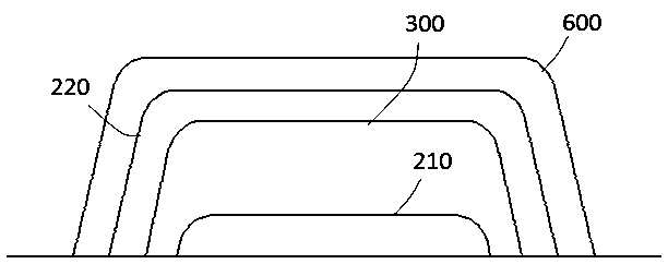
[0036] The implementation of the present invention will be described in detail below with reference to the accompanying drawings and embodiments, so as to fully understand how the present invention applies technical means to solve technical problems and achieve the realization process of technical effects and implement them accordingly. It should be noted that, as long as there is no conflict, each embodiment of the present invention and each feature in each embodiment can be combined with each other, and the technical solutions formed are all within the protection scope of the present invention.

[0037] It should be understood that the terms used in the present invention are only for the purpose of describing specific embodiments, and are not intended to limit the present invention. It is further understood that when the terms "comprising" and "including" are used in the present invention, they are used to indicate the existence of the stated features, wholes, steps, components,...


PUM

PropertyMeasurementUnit
Lengthaaaaaaaaaa
Widthaaaaaaaaaa
Thicknessaaaaaaaaaa

Abstract

The invention discloses a light emitting diode, which comprises a first electrode connected with a first semiconductor layer and a second electrode connected with a second semiconductor layer, whereinthe first electrode and/or the second electrode sequentially comprise/comprises a first reflecting layer, a connecting cushion layer and a second reflecting layer at least partially coating the connecting cushion layer, the material of the second reflecting layer comprises rhodium, platinum or ruthenium, and the first reflecting layer and the second reflecting layer are manufactured into a large-angle electrode structure through good stress characteristics, so that the photoelectric characteristics of the light-emitting diode is facilitated to be improved, and the product reliability is improved.

Description

technical field [0001] The invention relates to the field of semiconductor manufacturing, in particular to a light-emitting diode with high-reliability electrodes. Background technique [0002] see figure 1 In consideration of the light extraction efficiency, the electrode structure design of the existing LED chip adds a high-reflectivity material to the electrode structure as the reflective layer 200 to improve light efficiency, but most of the high-reflective materials: such as silver, aluminum, etc., have poor characteristics. The stability of the product is reduced by the influence of the environment, temperature, humidity, pH, etc., so a metal protection layer 230 with low mobility is covered for protection, but this design can only prolong the reaction time of the reflective layer material and the environment, and cannot completely Avoid major abnormalities such as metal material migration or precipitation and electrode shedding, which will cause the terminal product ...

Claims


Application Information

Patent Timeline
IPC IPC(8): H01L33/38H01L33/40H01L33/00
CPCH01L33/007H01L33/0075H01L33/38H01L33/405H01L2933/0016
Inventor 陈柏羽邓有财张中英
Owner XIAMEN SANAN OPTOELECTRONICS CO LTD
Why Eureka
Try Eureka