A kind of ultraviolet photoelectric device and preparation method thereof

A technology of electrical devices and ultraviolet light, which is applied in electrical components, photovoltaic power generation, semiconductor devices, etc., can solve the problems of low hole transport efficiency and strong ultraviolet absorption

Active Publication Date: 2021-07-27
GUANGDONG INST OF SEMICON IND TECH
View PDF5 Cites 0 Cited by
  • Summary
  • Abstract
  • Description
  • Claims
  • Application Information

AI Technical Summary

Problems solved by technology

[0004] The purpose of the present invention is to provide an ultraviolet photoelectric device and its preparation method, aiming to solve the problems of low hole transport efficiency and strong ultraviolet absorption in the existing p-type preparation technology of ultraviolet photoelectric devices

Method used


Image

  • A kind of ultraviolet photoelectric device and preparation method thereof
  • A kind of ultraviolet photoelectric device and preparation method thereof
  • A kind of ultraviolet photoelectric device and preparation method thereof

Examples


no. 1 example

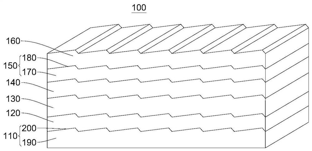
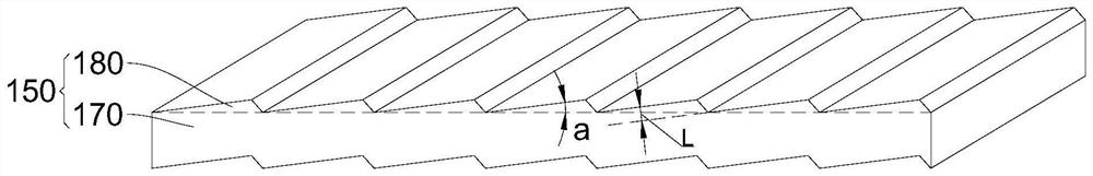
[0033] see figure 1 with figure 2 , the present embodiment provides an ultraviolet optoelectronic device 100, the ultraviolet optoelectronic device 100 includes a substrate 110 and a substrate 120 sequentially grown on the substrate 110, an n-type AlGaN layer 130, an active region 140, a p-type AlGaN layer 150 and contact layer 160. Wherein, the p-type AlGaN layer 150 includes a first body 170 and a first step 180 located on the top surface of the first body 170, a plurality of first steps 180 are periodically arranged in sequence, and the vertical height of the first step 180 is Straight section is triangular.

[0034] The drop distance L between two adjacent first steps 180 is greater than the thickness of the monoatomic layer. The drop distance L between two adjacent first steps 180 refers to the distance between the top surfaces of two adjacent first steps 180 , and of course the top surfaces of two adjacent first steps 180 are parallel to each other. It can also be s...

no. 2 example

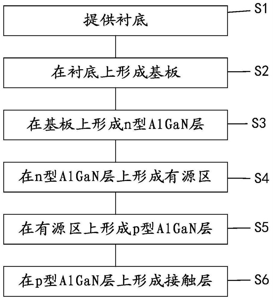
[0044] see image 3 , this embodiment provides a method for manufacturing the ultraviolet photoelectric device 100, which is mainly used for preparing the ultraviolet photoelectric device 100 in the first embodiment. The preparation method includes sequentially growing a substrate 120, an n-type AlGaN layer 130, an active region 140 and a p-type AlGaN layer 150 on a substrate 110; wherein the p-type AlGaN layer 150 includes a first body 170 and is located at the second For the first steps 180 on the top surface of a body 170 , the drop distance L between two adjacent first steps 180 is greater than the thickness of a monoatomic layer.

[0045] Specifically, the following steps are included:

[0046] S1: providing a substrate 110 .

[0047] The material of the substrate 110 is sapphire, and the substrate 110 is placed in the reaction chamber of the growth equipment. The growth equipment can be any one of metal-organic chemical vapor deposition, hydride vapor deposition, and m...


PUM


Abstract

The invention provides an ultraviolet photoelectric device and a preparation method thereof, which relate to the technical field of semiconductors. The ultraviolet photoelectric device includes a substrate, a substrate grown sequentially on the substrate, an n-type AlGaN layer, an active region, and a p-type AlGaN layer; the p-type AlGaN layer includes a first body and is located on the first For the first step on the top surface of the body, the drop distance L between two adjacent first steps is greater than the thickness of the monoatomic layer. The ultraviolet photoelectric device and its preparation method can stack a plurality of single atoms in the direction of the difference between two adjacent first steps, and form a step bunching effect on the p-type AlGaN layer, thereby increasing the number of holes Transport efficiency and weaken the ultraviolet absorption, improve the photoelectric conversion efficiency of the device.

Description

technical field [0001] The invention relates to the technical field of semiconductors, in particular to an ultraviolet photoelectric device and a preparation method thereof. Background technique [0002] Aluminum-gallium-nitride (AlGaN)-based ultraviolet optoelectronic devices have important application value in the fields of industrial curing, sterilization, non-line-of-sight communication, toxic gas detection, space charge processing, high-density data storage, and missile detection. However, the photoelectric conversion efficiency of current ultraviolet photoelectric devices is still very low, which is difficult to meet the application requirements of high-end products. In addition to the problem of material defects, the hole transport efficiency of AlGaN with high Al composition is low, which is another major problem faced by ultraviolet optoelectronic devices. The lower hole transport efficiency of AlGaN with high Al composition is due to the rapid decrease in the inco...

Claims


Application Information

Patent Timeline
Patent Type & Authority Patents(China)
IPC IPC(8): H01L31/0236H01L31/0352H01L31/103H01L31/18
CPCH01L31/02363H01L31/0352H01L31/1035H01L31/1848Y02E10/544Y02P70/50
Inventor 何晨光赵维吴华龙陈志涛张康贺龙飞刘云洲廖乾光
Owner GUANGDONG INST OF SEMICON IND TECH
Why Eureka
Try Eureka