Crystal back preparation method of ultrathin chip

An ultra-thin chip, chip technology, applied in the direction of semiconductor/solid-state device manufacturing, semiconductor devices, electrical components, etc., can solve the problems of unevenness, small contact area, thin thickness, etc., to achieve easy progress control, uniform cracks, and increased resistance. Effect

Pending Publication Date: 2020-04-28
闳康技术检测(上海)有限公司
View PDF6 Cites 0 Cited by
  • Summary
  • Abstract
  • Description
  • Claims
  • Application Information

AI Technical Summary

Problems solved by technology

[0004] However, due to the small contact area and thin thickness on the back of the ultra-thin chip, the direct grinding method will cause cracks on the back of the sample and uneven grinding, making the success rate of chip analysis very low

Method used


Image

  • Crystal back preparation method of ultrathin chip
  • Crystal back preparation method of ultrathin chip
  • Crystal back preparation method of ultrathin chip

Examples


Embodiment Construction

[0037] The present invention will be described in detail below in conjunction with the accompanying drawings and embodiments.

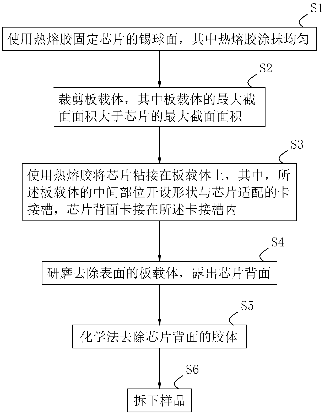
[0038] A method for preparing the crystal back of an ultra-thin chip, such as figure 1 shown, including the following steps:

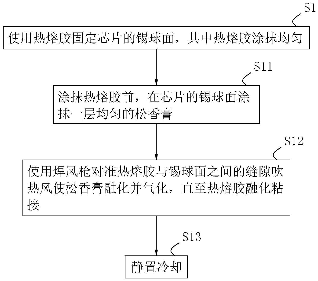
[0039] S1: Use hot melt adhesive to fix the solder spherical surface of the chip, and the hot melt adhesive is evenly applied. Such as figure 2 As shown, S1 also includes: S11: Before applying hot melt adhesive, apply a layer of rosin paste evenly on the solder ball surface of the chip. S12: Use a welding air gun to blow hot air at the gap between the hot melt adhesive and the solder ball surface to melt and vaporize the rosin paste until the hot melt adhesive is melted and bonded. S13: Stand to cool.

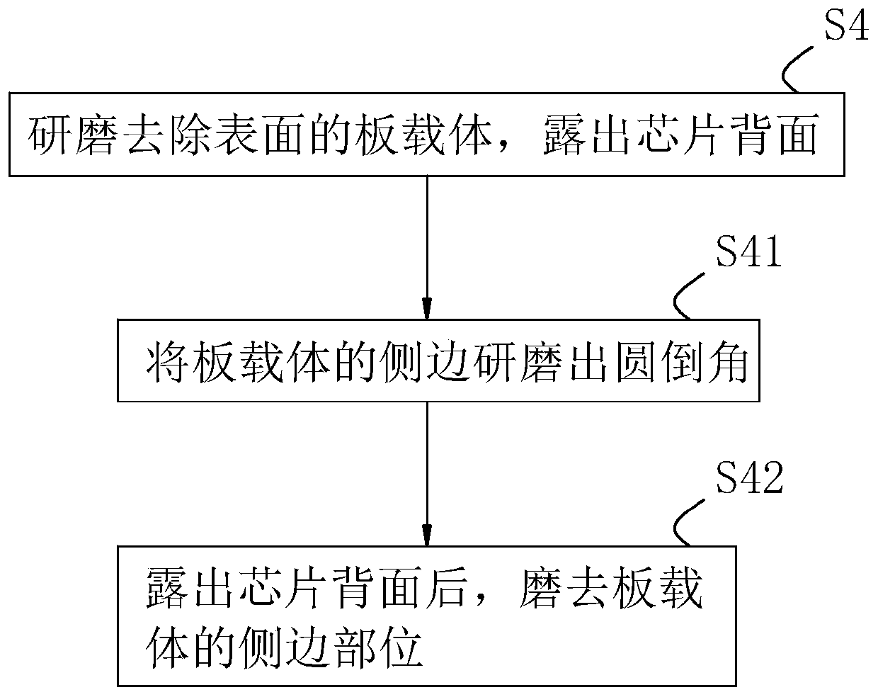
[0040] back to figure 1 , S2: Cutting the board carrier, wherein the maximum cross-sectional area of ​​the board carrier is larger than the maximum cross-sectional area of ​​the chip. The board carrier can use a PCB boar...


PUM


Abstract

The invention relates to the technical field of chip analysis and discloses a crystal back preparation method of an ultrathin chip. The method comprises the following steps that: S1, a the tin spherical surface of the chip is fixed by using a hot melt adhesive which is uniformly smeared; S2, a board carrier is cut, wherein the maximum cross-sectional area of the board carrier is greater than the maximum cross-sectional area of the chip; S3, the chip is bonded to the board carrier through the hot melt adhesive, a clamping groove shaped to match with the chip is formed in the middle of the boardcarrier, and the back face of the chip is clamped in the clamping groove; S4, the board carrier on the surface is ground so as to be removed, so that the back surface of the chip can be exposed; S5,the adhesive on the back surface of the chip is removed by a chemical method; and S6, a sample is removed. In the grinding process, borne force can be evenly distributed by the board carrier; meanwhile, the board carrier can increase grinding resistance, and therefore, the progress of the grinding can be more easily controlled when thickness is reduced, grinding uniformity and quality are improved, cracks cannot occur on the back surface of the chip, and the grinding is more uniform.

Description

technical field [0001] The invention relates to the technical field of chip analysis, more specifically, it relates to a crystal back preparation method of an ultra-thin chip. Background technique [0002] Even if the circuit simulation software continues to improve and evolve, it is still difficult to ensure the correctness of the chip design and layout 100%. Once a circuit defect is found, the mask can only be revised again; however, the mask is expensive, and after the mask is reloaded, The wait time for a patched chip is usually more than a month. Therefore, most IC design companies will choose to conduct IC circuit analysis and repair, which can be completed within a few hours to ensure that the circuit design meets expectations and reduce the cost of time and money. [0003] When analyzing and repairing the chip, it is necessary to prepare the crystal back, which is the back of the IC chip. The existing crystal back preparation method is cross-section or crystal back...

Claims


Application Information

Patent Timeline
Patent Type & Authority Applications(China)
IPC IPC(8): H01L21/683H01L21/304
CPCH01L21/6835H01L21/304H01L2221/68327
Inventor 高峰黄勇超林廷伟
Owner 闳康技术检测(上海)有限公司
Why Eureka
Try Eureka