
Array substrate and preparation method thereof

An array substrate and a substrate technology, which are applied in the field of array substrates and their preparation, can solve the problem that the brightness uniformity of the screen cannot be improved, etc.

Inactive Publication Date: 2020-05-05
WUHAN CHINA STAR OPTOELECTRONICS SEMICON DISPLAY TECH CO LTD
View PDF5 Cites 2 Cited by
  • Summary
  • Abstract
  • Description
  • Claims
  • Application Information

AI Technical Summary

Problems solved by technology

[0003] In order to solve the above technical problems, the present invention provides an array substrate and its preparation method to solve the technical problem that the brightness uniformity of the screen cannot be improved in the prior art

Method used


Image

  • Array substrate and preparation method thereof
  • Array substrate and preparation method thereof
  • Array substrate and preparation method thereof

Examples


Embodiment 1

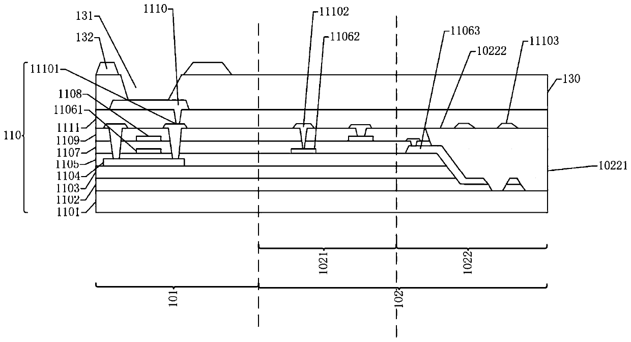
[0095] In this embodiment, the array substrate of the present invention includes a thin film transistor layer 110 , an anode layer 120 and a pixel definition layer 130 .

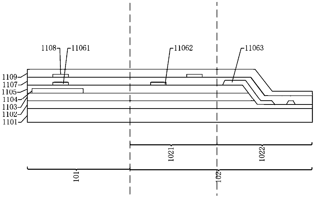
[0096] Such as figure 1 As shown, wherein, the thin film transistor layer 110 includes a substrate 1101, a barrier layer 1102, a buffer layer 1103, an active layer 1104, a first insulating layer 1105, a first gate layer 1106, a second insulating layer 1107, a second gate An electrode layer 1108 , a third insulating layer 1109 , a source-drain electrode layer 1110 and a planar layer 1111 .

[0097] The barrier layer 1102 is provided on the substrate 1101, and the material used for the barrier layer 1102 includes one or more of silicon oxide, silicon nitride, silicon oxynitride and amorphous silicon, and is mainly used to block water and oxygen. , preventing water and oxygen from corroding the array substrate.

[0098] The buffer layer 1103 is disposed on the barrier layer 1102, and the buffer layer 1103 is ...

Embodiment 2

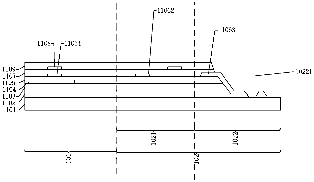
[0139] Such as Figure 5 As shown, in this embodiment, the structure of the array substrate of the present invention is generally similar to that of the array substrate in Embodiment 1, the difference is that the second gate layer 1108 in the array substrate in this embodiment includes The fourth metal segment 11081 , the fifth metal segment 11082 and the sixth metal segment 11083 .

[0140] The fourth metal segment 11081 is disposed on the second insulating layer 1107 in the display area 101 and corresponds to the active layer 1104 . The fifth metal segment 11082 is disposed in the fan-out region 1021, the sixth metal segment 11083 is disposed in the bonding region 1022, wherein the first gate layer 1106 is disposed in the first on the insulating layer 1105 and corresponding to the second gate layer 1108 .

[0141] An opening 10221 is provided in the bonding region 1022, and the opening 10221 penetrates through the third insulating layer 1109, the second insulating layer 11...


PUM


Abstract

The invention discloses an array substrate and a preparation method thereof. The array substrate comprises a display area and a non-display area. The non-display area is provided with a bonding area and a fan-out area. The fan-out area is arranged between the display area and the bonding area. The array substrate further comprises a thin film transistor structure layer which comprises a grid electrode layer and a source-drain electrode layer. The grid electrode layer and the source-drain electrode layer are made of at least one of titanium, aluminum and titanium-aluminum alloy. The array substrate and the preparation method thereof, which are provided by the invention, have the beneficial effects that the grid electrode layer and the source-drain electrode layer on the array substrate aremade of the same material such as low-resistance and bending-resistant metal such as aluminum, titanium and titanium-aluminum alloy; the conductivity and the bending characteristic of metal wires areimproved; in the bonding area of the array substrate, the grid electrode layer is arranged below an organic layer and is closer to a neutral surface, and thus the risk of wire breakage of the bondingarea is reduced; and the grid electrode layer is used as a mask plate for inorganic film layer patterning, which saves the cost , and meanwhile solves the problem that adhesion of metal wires to the etched flexible substrate is poor.

Description

technical field [0001] The invention relates to the display field, in particular to an array substrate and a preparation method thereof. Background technique [0002] OLED (Organic Light-Emitting Diode) is widely used due to its light weight, self-illumination, wide viewing angle, low driving voltage, high luminous efficiency, low power consumption, and fast response, especially flexible OLED display devices. The characteristics of being bendable and easy to carry have become the main field of research and development in the field of display technology. At present, high-end mobile phones have high requirements on brightness uniformity. How to improve the brightness uniformity of the screen is the key direction of the development of major manufacturers. Contents of the invention [0003] In order to solve the above technical problems, the present invention provides an array substrate and a preparation method thereof, which are used to solve the technical problem that the b...

Claims


Application Information

Patent Timeline
Patent Type & Authority Applications(China)
IPC IPC(8): H01L27/12H01L21/77H01L27/32G09F9/30
CPCH01L27/1214H01L27/1259H01L27/1244H01L27/1288H01L21/77G09F9/301H10K59/12
Inventor 陈诚
Owner WUHAN CHINA STAR OPTOELECTRONICS SEMICON DISPLAY TECH CO LTD
Learn More