Level-triggered D flip-flop circuit based on resistive memory

A memory and flip-flop technology, which is applied to parts, electrical components, and electric pulse generation of electric pulse circuits, can solve the problems of insufficient layout area advantage and insufficient refinement of circuit structure, etc., and achieve layout area advantage and simple structure , the effect of large layout area

Pending Publication Date: 2020-05-08
SUZHOU UNIV
View PDF0 Cites 2 Cited by
  • Summary
  • Abstract
  • Description
  • Claims
  • Application Information

AI Technical Summary

Problems solved by technology

[0003] The above circuit utilizes the non-volatile characteristics of the memristor and the compatibility between the memristor and the CMOS process to complete the design of the level-triggered D flip-flop, but compared with the level-triggered D flip-flop of the traditional CMOS proce...

Method used


Image

  • Level-triggered D flip-flop circuit based on resistive memory
  • Level-triggered D flip-flop circuit based on resistive memory
  • Level-triggered D flip-flop circuit based on resistive memory

Examples


Embodiment 1

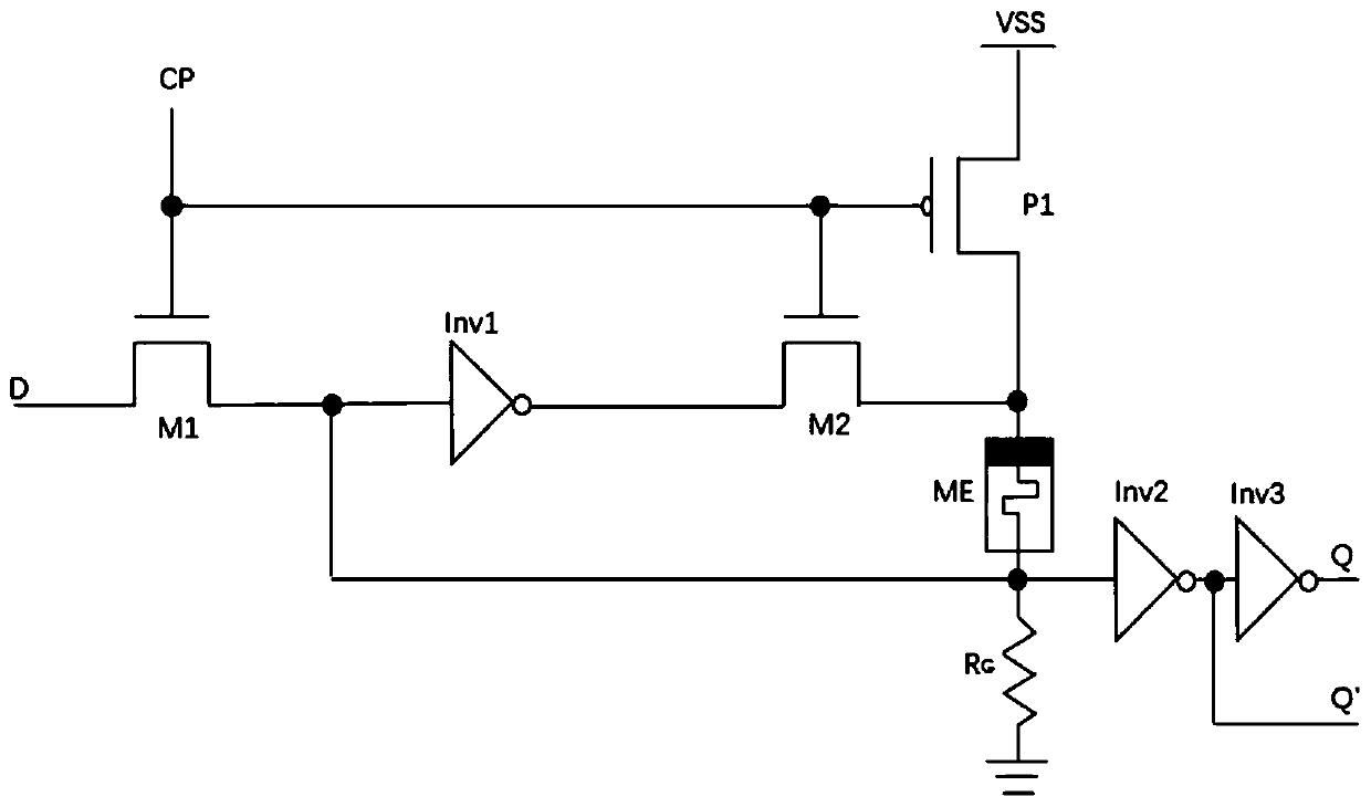
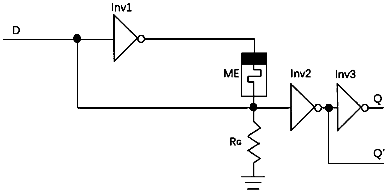
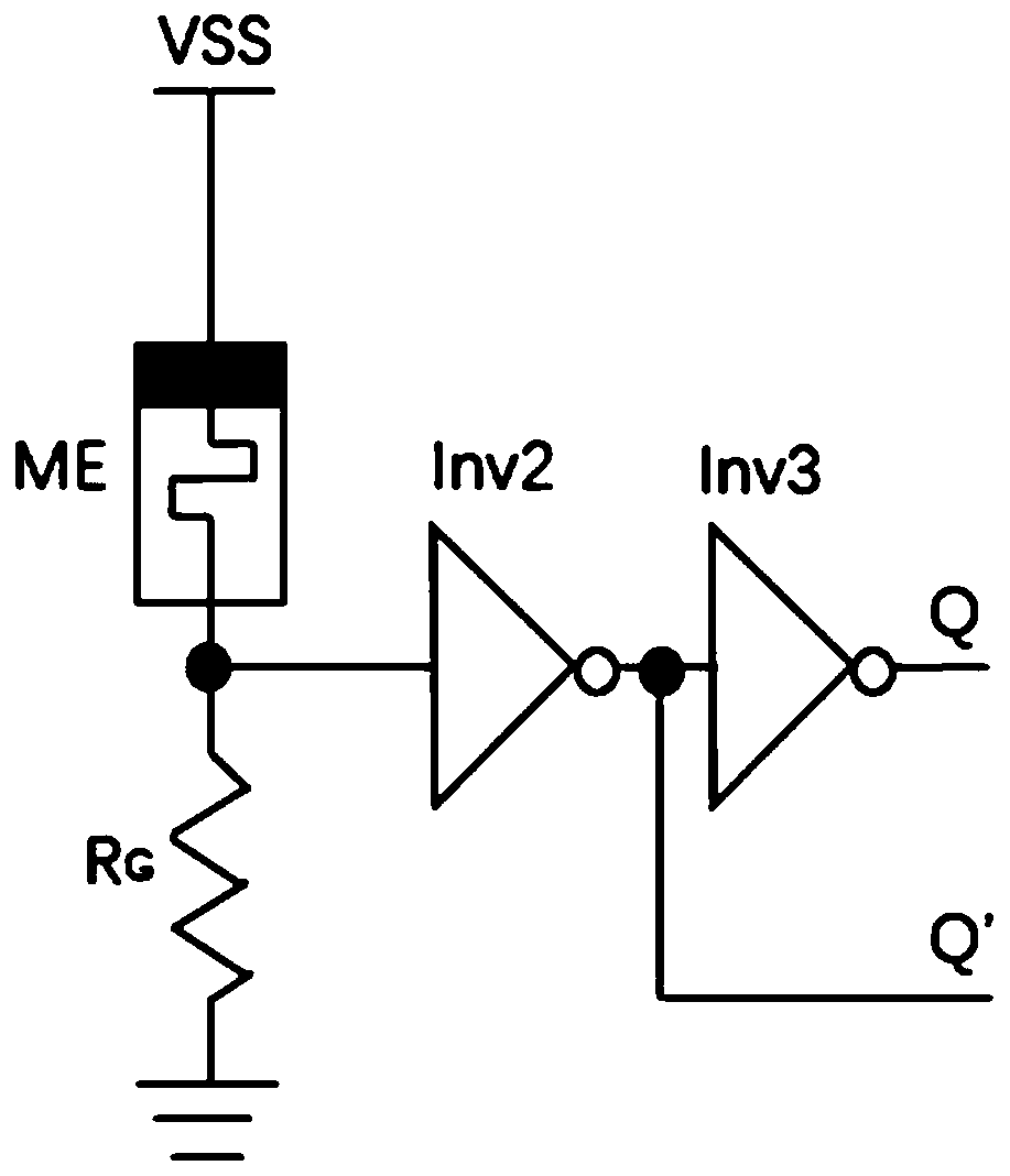
[0031] see Figure 4 As shown, the present invention relates to a level-triggered D flip-flop circuit based on resistive memory, comprising a MOSFET tube M1, a first memristor ME1, a resistor R G , the first inverter INV1 and the second inverter INV2;

[0032] The source of the MOSFET M1 is electrically connected to the input signal D, the gate of the MOSFET M1 is electrically connected to the clock pulse signal CP, and the drains of the MOSFET M1 are respectively electrically connected to the first memristor ME1 positive pole, resistor R G One terminal of the first inverter INV1 and the input terminal of the first inverter INV1, the output terminal of the first inverter INV1 is electrically connected to the input terminal of the second inverter INV2, and the output terminal of the second inverter INV2 is electrically The negative pole of the first memristor ME1 is electrically connected to the output terminal of the NAND logic circuit for auxiliary setting thereof, and one ...

Embodiment 2

[0046] see Figure 10 As shown, the present invention also relates to another level-triggered D flip-flop circuit based on resistive memory, including a MOSFET tube M1, a first memristor ME1, a resistor R G , the first inverter INV1, the second inverter INV2 and the fourth inverter INV4;

[0047] The source of the MOSFET M1 is electrically connected to the input signal D, the gate of the MOSFET M1 is electrically connected to the output terminal of the fourth inverter INV4, and the input terminal of the fourth inverter INV4 is electrically connected to The clock pulse signal CP, the drain of the MOSFET M1 is electrically connected to the anode of the first memristor ME1 and the resistor R G One terminal of the first inverter INV1 and the input terminal of the first inverter INV1, the output terminal of the first inverter INV1 is electrically connected to the input terminal of the second inverter INV2, and the output terminal of the second inverter INV2 is electrically The ne...


PUM


Abstract

The invention discloses a level triggered D flip-flop circuit based on a resistive memory. The level triggered D flip-flop circuit comprises an MOSFET, a first memristor, a resistor, a first phase inverter and a second phase inverter. The source electrode of the MOSFET is electrically connected with an input signal; the grid electrode of the MOSFET is electrically connected with a clock pulse signal; the drain electrode of the MOSFET is electrically connected to the positive electrode of the first memristor, one end of the resistor and the input end of the first inverter. The output end of thefirst phase inverter is electrically connected to the input end of the second phase inverter; the output end of the second phase inverter is electrically connected with an output signal; the negativeelectrode of the first memristor is electrically connected to the output end of the NAND logic circuit used for conducting auxiliary setting on the first memristor, one input end of the NAND logic circuit is electrically connected with an input signal, the other input end of the NAND logic circuit is electrically connected with a clock pulse signal, and the other end of the resistor is grounded.According to the invention, the structure of the circuit is simpler and more refined, and the layout area has greater advantages.

Description

technical field [0001] The invention relates to the field of basic circuit design of an integrated circuit memory, in particular to a level-triggered D flip-flop circuit based on a resistive memory. Background technique [0002] Level-triggered D flip-flops, also known as D-type latches, are commonly used storage units in integrated circuits. figure 1 It is the circuit diagram of the memristor-based level-triggered D flip-flop in the past. Its working principle is: when the clock pulse CP is high level 1, M1 and M2 are turned on, and P1 is turned off. The equivalent circuit diagram is as follows figure 2 shown. At this time, if the input signal D is 1, the output signal Q is 1, and since a 1-setting (low resistance state of the memristor is "1") voltage Vset is applied to both ends of the memristor ME, the memristor is in In the low-impedance state, the resistance value is RL; if the input signal D is 0, the output signal Q is 0, and since a zero-setting voltage Vclear is...

Claims


Application Information

Patent Timeline
IPC IPC(8): H03K3/3562H03K3/01
CPCH03K3/01H03K3/3562
Inventor 张文海王子欧
Owner SUZHOU UNIV
Why Eureka
Try Eureka