3D NAND memory and manufacturing method thereof

A 3D NAND and manufacturing method technology, applied in the direction of electric solid-state devices, semiconductor devices, electrical components, etc., can solve the problems of poor uniformity of selective epitaxial structure, insufficient substrate cleanliness, incomplete cleaning, etc., and achieve easy control of the patterning process , Reduce the risk of leakage and save manufacturing costs

Inactive Publication Date: 2020-05-15
YANGTZE MEMORY TECH CO LTD
View PDF4 Cites 5 Cited by
  • Summary
  • Abstract
  • Description
  • Claims
  • Application Information

AI Technical Summary

Problems solved by technology

The process of this method is cumbersome, and the process of etching to form trenches will also cause damage to the substrate
When forming the storage structure, etch the stacked structure to form a channel hole, and then grow the selective epitaxial structure at the bottom of the channel hole. Before forming the selective epitaxial structure, the channel hole and the substrate need to be etched first. Cleaning, this cleaning process is easy to cause damage to the substrate, or the cleaning is not thorough, the substrate cleanliness is not enough, and the uniformity of the selective epitaxial growth structure is poor, etc.

Method used


Image

  • 3D NAND memory and manufacturing method thereof
  • 3D NAND memory and manufacturing method thereof
  • 3D NAND memory and manufacturing method thereof

Examples


Embodiment 1

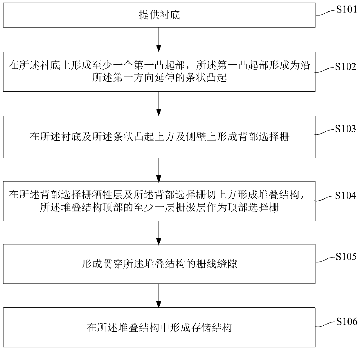
[0128] This embodiment provides a method for manufacturing a 3D NAND memory, such as figure 1 As shown, the method includes the following steps:

[0129] Step S101: providing a substrate;

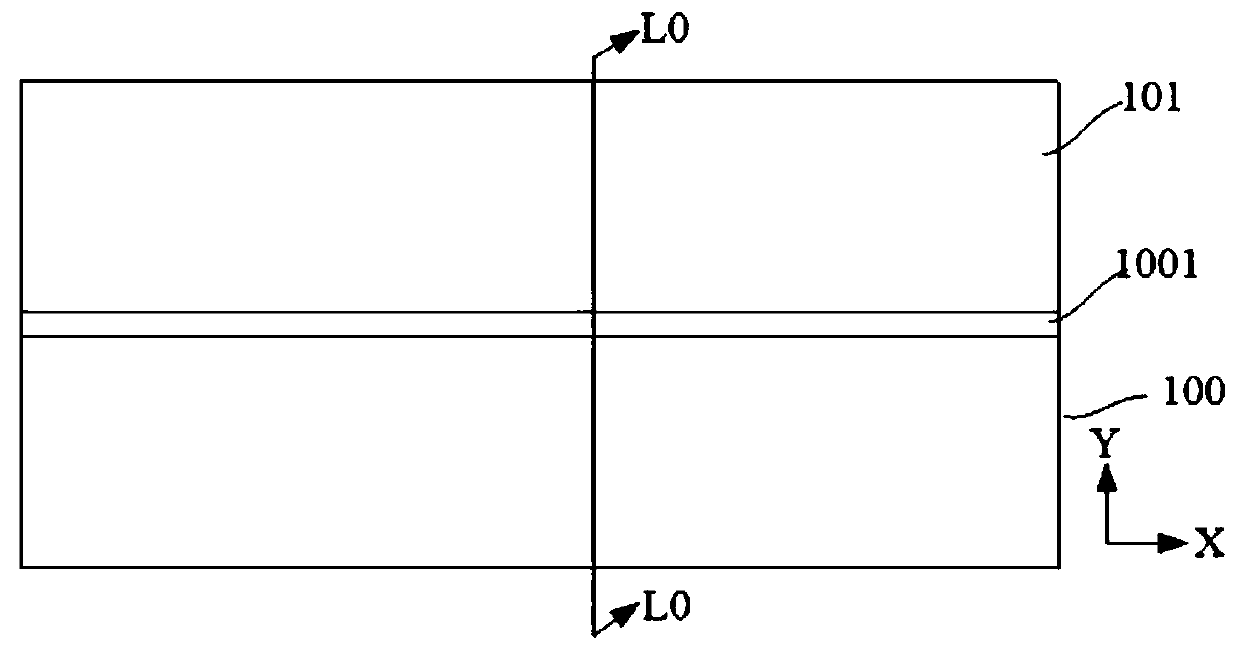
[0130] refer to figure 2 , a substrate 100 is provided, and the substrate 100 extends in the X direction (first direction) and the Y direction (second direction). The material of the substrate 100 can be single crystal silicon (Si), single crystal germanium (Ge), or silicon germanium (GeSi), silicon carbide (SiC); it can also be silicon on insulator (SOI), germanium on insulator (GOI ); or other materials, such as III-V group compounds such as gallium arsenide. In this embodiment, the material of the semiconductor substrate 100 is single crystal silicon (Si).

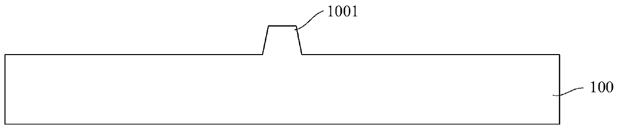
[0131] Step S102: forming at least one first raised portion on the substrate, the first raised portion being formed as a strip-shaped protrusion extending along the first direction;

[0132] Such as figure 2 and image 3 As ...

Embodiment 2

[0148] This embodiment also provides a method for manufacturing a 3D NAND memory. The similarities between the manufacturing method of this embodiment and the manufacturing method described in Embodiment 1 will not be repeated, and the differences are described in detail as follows:

[0149] refer to Figure 17 In this embodiment, a plurality of second protrusions 107 distributed in an array are formed on the substrate 100 at the same time as the first protrusions are formed on the patterned substrate 100 . Such as Figure 18 As shown, the second protrusions 107 are columnar protrusions distributed in an array. Preferably, the first raised portion and the second raised portion have the same height.

[0150]In a preferred embodiment of this embodiment, after the formation of the first protrusions, the substrate may be patterned again to form a plurality of second protrusions 107 . The second raised portion may be formed simultaneously or after the first raised portion may be...

Embodiment 3

[0161] This embodiment provides a kind of 3D NAND memory, refer to the attached figure 2 ~ attached Figure 15 , the 3D NAND memory includes:

[0162] A substrate 100, the substrate 100 extends in a first direction (X direction) and a second direction (Y direction) perpendicular to each other, the substrate 100 includes at least one first raised portion 102, the first raised portion 102 forms It is a strip-shaped protrusion extending along the X direction. The material of the substrate 100 can be single crystal silicon (Si), single crystal germanium (Ge), or silicon germanium (GeSi), silicon carbide (SiC); it can also be silicon on insulator (SOI), germanium on insulator (GOI) ; or other materials, such as III-V group compounds such as gallium arsenide. In this embodiment, the material of the semiconductor substrate 100 is single crystal silicon (Si).

[0163] A back selection gate formed on the substrate, the back selection gate comprising a back selection gate oxide and...


PUM


Abstract

The invention provides a 3D NAND memory and a manufacturing method thereof. The method comprises the following steps of: by etching a substrate, strip-shaped raised first raised parts are formed on the substrate; the back selection gate oxides formed on the upper portions and the side walls of the first raised parts form back selection gate tangent lines, the subsequently-formed back selection gates are cut off, separation control over the back selection gates is achieved, the control time of the device is prolonged, and the RC delay effect of a word line layer of the device is reduced. Or while the first raised part is formed, columnar raised second raised parts which are distributed in an array manner are formed on the substrate. The storage structures distributed in an array mode and formed in the stacking structure correspond to the second protruding parts in a one-to-one mode, and part of the storage structures are formed on the first raised parts. The first raised parts and the second raised parts replace a selective epitaxial structure formed in a channel hole, the substrate patterning process is easy to control, and etching post-processing is not needed.

Description

technical field [0001] The invention relates to the field of semiconductor integrated circuit manufacturing, in particular to a 3D NAND memory and a manufacturing method thereof. Background technique [0002] As the feature size of devices in integrated circuits continues to shrink, 3D memory technologies that stack multiple planes of memory cells to achieve greater storage capacity and lower cost per bit are increasingly favored. [0003] In 3D NAND memory, the top select gate of a stacked gate is usually used to control the memory structure. As the number of stacked layers increases, the storage structure is controlled respectively through the back selection gate and the top selection gate. However, as the number of stacked layers increases, when forming the tangent line of the back selection gate, it is usually used to first form part of the stacked layer, then etch part of the stacked layer to form a trench, and fill the trench with insulating material to form the tange...

Claims


Application Information

Patent Timeline
Patent Type & Authority Applications(China)
IPC IPC(8): H01L27/115H01L27/1157H01L27/11582
CPCH10B69/00H10B43/35H10B43/27
Inventor 肖梦耿静静张慧吴佳佳王攀
Owner YANGTZE MEMORY TECH CO LTD
Why Eureka
Try Eureka