Lithium niobate optical waveguide device and preparation method thereof

A technology of lithium niobate and optical waveguide, which is applied in the field of optical communication, can solve the problems of complex ion exchange process, increase transmission loss, and inability to effectively reduce loss, etc., achieve simple mask etching process, reduce transmission loss, increase the binding effect

Inactive Publication Date: 2020-05-19
UNIV OF ELECTRONICS SCI & TECH OF CHINA
View PDF5 Cites 9 Cited by
  • Summary
  • Abstract
  • Description
  • Claims
  • Application Information

AI Technical Summary

Problems solved by technology

[0005] In practical applications, due to the thickness of the substrate, the light will dissipate to the surroundings, thereby increasing the transmission loss, so it is necessary to thin the various tangential lithium niobate blocks. The current method is to mechanically reduce the thickness of the substrate. grinding, but the thickness of lithium niobate obtained by this method is still tens of microns, which cannot effectively reduce the loss; secondly, the ion exchange process is complicated and cannot be applied to all tangential lithium niobate, and the refraction of the upper and lower layers The rate difference is small and does not tie the beam well in the waveguide

Method used


Image

  • Lithium niobate optical waveguide device and preparation method thereof
  • Lithium niobate optical waveguide device and preparation method thereof
  • Lithium niobate optical waveguide device and preparation method thereof

Examples


Embodiment Construction

[0025] In order to make the purpose, technical solutions and advantages of the embodiments of the present invention clearer, the technical solutions in the embodiments of the present invention will be described in detail below in conjunction with the drawings in the embodiments of the present invention. Obviously, the described embodiments are the Some embodiments of the invention are not all embodiments. Based on the embodiments of the present invention, all other embodiments obtained by those of ordinary skill in the art without creative efforts belong to the protection scope of the present invention.

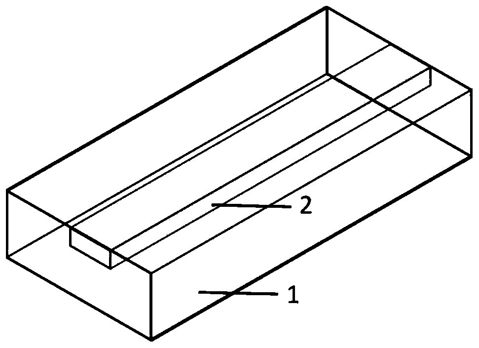
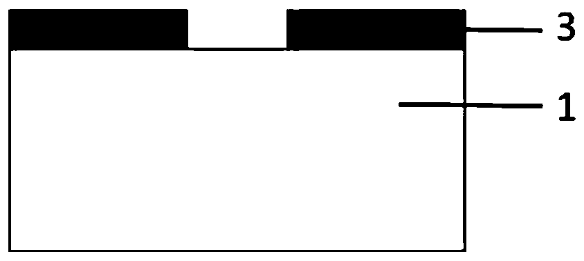
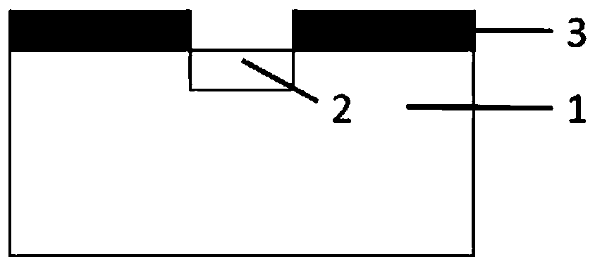
[0026] figure 1 It is a three-dimensional schematic diagram of a lithium niobate optical waveguide made by the prior art; Figure 2 to Figure 4 It is a schematic diagram of the technological process of manufacturing the lithium niobate optical waveguide using the prior art. The process of manufacturing lithium niobate optical waveguide in the prior art is as follows: first, ...


PUM

PropertyMeasurementUnit
thicknessaaaaaaaaaa
lengthaaaaaaaaaa
refractive indexaaaaaaaaaa

Abstract

The invention relates to a preparation method of a lithium niobate optical waveguide device, and belongs to the technical field of optical communication. According to the invention, a new cladding structure is introduced, a micron-order lithium niobate thin film optical waveguide device is obtained through the processes of ion implantation, BCB spin coating, bonding, annealing and the like, the preparation of a ridge waveguide is facilitated in process, the transmission loss of a finally prepared optical waveguide is effectively reduced, and the constraint of light is increased. According to the invention, a BCB is selected as a bonding medium material and used as an adhesive at normal temperature, so that a lithium niobate film and a substrate can be effectively combined together, the BCBis cured after annealing and used as a waveguide cladding, the subsequent mask etching process of a lithium niobate thin film is simple and convenient, and the lithium niobate thin film is not damaged; the optical refractive index of lithium niobate is 2.2, is greater than the refractive index 1.5 of the BCB and is greater than the refractive index 1 of air, and light can be well restrained in the waveguide, so that excellent performance can be realized without proton exchange.

Description

technical field [0001] The invention relates to a lithium niobate optical waveguide device and a preparation method thereof, belonging to the technical field of optical communication. Background technique [0002] Lithium niobate crystal has excellent electro-optic, acousto-optic and nonlinear properties, and the material has stable chemical properties. It is the most commonly used inorganic dielectric crystal material for integrated optics and is widely used in the preparation of various optical waveguide devices in the field of optical communication. By changing the structure of lithium niobate optical waveguides and electrodes, a variety of optical transmission and control devices can be prepared, such as optical waveguides, electro-optical modulators, and microring resonators. [0003] In order to make a waveguide, it is necessary to fabricate SiO on the upper surface of the substrate 2 or Si 3 N 4 thin film, and then etched the mask window by photolithography technol...

Claims


Application Information

Patent Timeline
Patent Type & Authority Applications(China)
IPC IPC(8): G02B6/12G02B6/122
CPCG02B6/12G02B6/122G02B2006/1204G02B2006/12169G02B2006/12188
Inventor 帅垚高琴吴传贵罗文博乔石珺张万里
Owner UNIV OF ELECTRONICS SCI & TECH OF CHINA
Why Eureka
Try Eureka